Past exam of the MPhil in micro- and nanotechnology enterprise course of the University of Cambridge 2017 Paper 2 Section B 22 i Solution by  Codex 0 2026-10-20
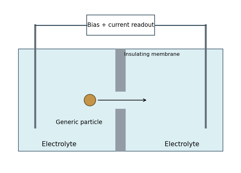
In generic resistive-pulse sensing, two electrolyte reservoirs are connected through a small aperture. Electrodes apply a bias and a low-noise current amplifier records the pore current. Passage of a weakly charged insulating particle excludes conducting liquid, usually increasing resistance and giving a transient current decrease at fixed voltage. Pulse amplitude, duration and event rate contain size-, transport- and concentration-dependent information, subject to calibration.
Advantages include label-free single-particle counting, electrical readout and small active volume. Limitations include clogging, electrode/pore noise, finite bandwidth, uncertain particle trajectories and surface-conduction effects; a pulse is not intrinsically chemically specific. Strong particle charge or concentration polarization can complicate, or even reverse, the simple blockade signal. The schematic below uses only generic nonbiological particle transport.
Past exam of the MPhil in micro- and nanotechnology enterprise course of the University of Cambridge 2017 Paper 2 Section B 21 iv Solution by Codex 0 2026-10-20
Codex 0 2026-10-20The intended double-barrier resonant-tunnelling diode has a bias-dependent well level. Initially increasing bias can bring a quasi-bound level into alignment with available occupied emitter states, sharply increasing current. At larger bias the resonant level moves out of the effective injection window, for example below the emitter conduction-band edge, so resonant transmission and current decrease despite increasing voltage. This produces a peak-to-valley interval with . Further bias can increase nonresonant or higher-level current again.
The right panel of the preceding figure is a qualitative example. The device can supply small-signal negative differential conductance to an appropriate oscillator circuit while its current and voltage remain positive. A bias-independent transmission function alone does not guarantee NDR: the voltage-dependent potential profile, contacts and carrier supply must be included. The source's reference to part (ii) appears to point to the earlier barrier matching; the resonant device mechanism uses the added barrier of part (iii).
Past exam of the MPhil in micro- and nanotechnology enterprise course of the University of Cambridge 2017 Paper 2 Section B 21 iii Solution by Codex 0 2026-10-20
Codex 0 2026-10-20Between two barriers, region III becomes a finite intermediate well containing both right- and left-moving oscillatory components, . Repeated reflection produces standing-wave-like enhancement and quasi-bound levels with finite escape lifetimes. At resonant energies, the multiple transmitted amplitudes add constructively: an ideal symmetric lossless pair can have transmission approaching unity even when a single barrier transmits poorly. Away from resonance the pair strongly suppresses transmission.
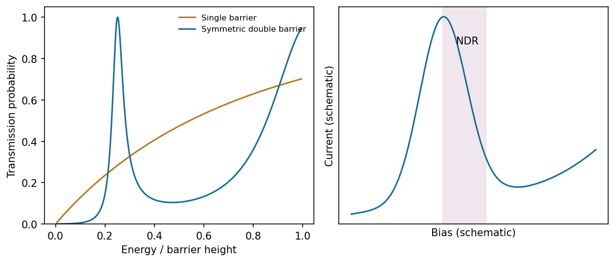
Calculated single- and double-barrier transmission and a separate qualitative resonant-tunnelling current-voltage characteristic
. Source. Details. A useful phase condition is , where is the intermediate-well width and the reflection phases account for penetration into the barriers. The printed figure starts the second barrier at , so its well width is ; if the prose's second-barrier position is used instead, the width is . The resonance argument is unchanged once that geometrical convention is fixed.
Past exam of the MPhil in micro- and nanotechnology enterprise course of the University of Cambridge 2017 Paper 2 Section B 21 ii Solution by Codex 0 2026-10-20
Codex 0 2026-10-20For a finite potential step and constant mass, and are continuous. A finite jump of would require a delta-function contribution in the integrated equation, while a jump of would be still more singular. Matching the preceding amplitudes givesThe transmission probability is because the incident and transmitted regions have equal wave vector and mass; in unequal leads a velocity ratio is also required. These matching conditions do not apply unmodified to infinite walls, delta barriers or mass discontinuities.
Past exam of the MPhil in micro- and nanotechnology enterprise course of the University of Cambridge 2017 Paper 2 Section B 21 i Solution by Codex 0 2026-10-20
Codex 0 2026-10-20Take and equal electron mass in all regions. Define and . ThenThere is no wave incident from the far right. Region I contains oscillatory incident and reflected waves; region II is evanescent, with real exponentials rather than propagating plane waves. Both exponential terms are allowed in a finite barrier; deleting the growing term before boundary matching is generally incorrect. A complex superposition in the barrier can carry a nonzero conserved tunnelling current.
Past exam of the MPhil in micro- and nanotechnology enterprise course of the University of Cambridge 2017 Paper 2 Section B 20 v Solution by Codex 0 2026-10-20
Codex 0 2026-10-20For a tube, . A cut normal to its axis crosses ten axial load-bearing C-C bonds in the ideal unstrained honeycomb geometry. Assuming equal load sharing and simultaneous failure at per bond,The graphene areal mass is , giving linear mass densitysince the tex unit has . Thus the ideal carbon nanotube tenacity isThis neglects vacancies, curvature-induced changes in bond strength, thermal activation, imperfect load sharing and structural relaxation at failure. An aligned macroscopic fibre is a network of finite tubes or bundles: sliding, weak intertube shear transfer, imperfect alignment, defects and unequal load participation limit its strength. The nominal fibre diameter alone does not turn it into one defect-free covalent cylinder, explaining why a value near can be much lower than this ideal single-tube estimate.
Past exam of the MPhil in micro- and nanotechnology enterprise course of the University of Cambridge 2017 Paper 2 Section B 20 iv Solution by Codex 0 2026-10-20
Codex 0 2026-10-20The real-space carbon honeycomb has two atoms in a primitive cell of its triangular Bravais lattice. The reciprocal lattice is also triangular, and its Wigner-Seitz cell is a hexagonal first Brillouin zone. With a consistent orientation convention, the reciprocal-zone hexagon is rotated by relative to a real-space carbon-ring hexagon; reciprocal lengths scale inversely with the direct lattice spacing.
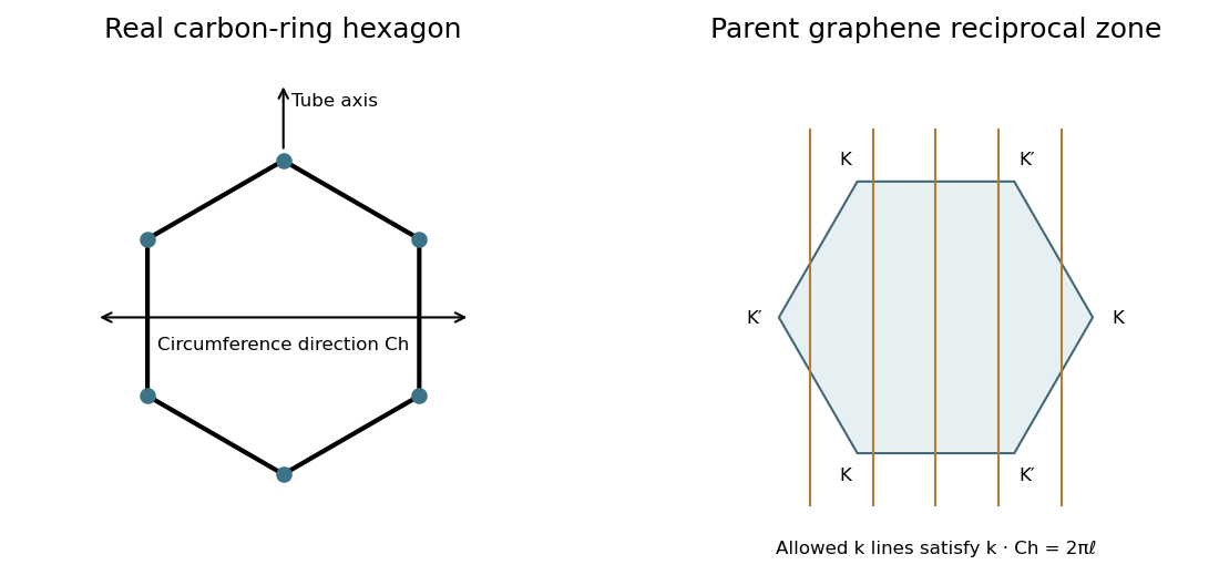


Rolling into a tube imposes , leaving parallel allowed lines in graphene's two-dimensional reciprocal space. They run along the tube-axis direction, perpendicular to the circumferential wrapping vector. The nanotube's actual one-dimensional Brillouin zone is an interval of axial wave vectors with period , where is its axial translation. The parent hexagon is therefore a zone-folding construction, not a literal two-dimensional Brillouin zone for the finished one-dimensional tube.
Past exam of the MPhil in micro- and nanotechnology enterprise course of the University of Cambridge 2017 Paper 2 Section B 20 iii Solution by Codex 0 2026-10-20
Codex 0 2026-10-20Each concentric shell has a different circumference, so it generally needs a different integer wrapping vector . Different vector lengths do not force different chiral angles, but exact atomic registry between all curved shells is geometrically restrictive. The shells can nucleate with different wrapping orientations, and strong covalent bonding within each shell dominates the weaker intershell interaction.
Consequently, it is usually unnecessary to strain every shell into a common orientation and registry; many multiwall tubes have incommensurate shells with different chiral angles. Identical chiral angles are possible, for example among suitable members of one armchair family, and should not be ruled out purely because the radii differ. Atomic indices, chiral angle and interwall commensurability are distinct descriptions.
Past exam of the MPhil in micro- and nanotechnology enterprise course of the University of Cambridge 2017 Paper 2 Section B 20 ii Solution by Codex 0 2026-10-20
Codex 0 2026-10-20The circumference is the length of the graphene wrapping vector:For ,Approximating the closest wall-to-wall separation by the graphite interlayer spacing gives the nearest-neighbour axis separation in a triangularly packed bundle:This assumes undeformed circular tubes with a graphitic contact gap. Faceting, flattening, adsorbates or pressure can alter a real bundle's spacing.
Past exam of the MPhil in micro- and nanotechnology enterprise course of the University of Cambridge 2017 Paper 2 Section B 20 i Solution by Codex 0 2026-10-20
Codex 0 2026-10-20In floating-catalyst CNT growth, a controlled sulfur additive acts as a growth promoter for the catalyst, commonly iron. Sulfur modifies catalyst surface composition, carbon uptake and the strength of the catalyst-carbon interaction; it can facilitate cap formation/lift-off and sustained tube growth instead of complete catalyst encapsulation. It also changes catalyst-particle evolution and hence tube yield, diameter and wall-count distributions.
There is an optimum range: excessive sulfur can occupy active sites or form an insufficiently active sulfide-rich catalyst and reduce growth. The additive is not simply a constituent that must be incorporated into every carbon wall. Its detailed action depends on catalyst, carbon source and process conditions; a single universal melting-point explanation is insufficient.[ref]
The promoter role of sulfur in carbon nanotube growth by Balázs Orbán and Tibor Höltzl. First-principles evidence for sulfur weakening iron-carbon binding; later mechanistic support, not an official answer
Past exam of the MPhil in micro- and nanotechnology enterprise course of the University of Cambridge 2017 Paper 2 Section A(iii) 19 iv Solution by Codex 0 2026-10-20
Codex 0 2026-10-20Relative to conventional crystalline-silicon technology, many organic absorbers offer low-temperature thin-film processing and lightweight flexible devices, but have more strongly bound excitons and more disorder-limited charge transport. These are common material trends, not universal statements about every organic or inorganic device.
Relevant semiconductor properties include the absorption spectrum and optical gap, donor/acceptor energy levels and offsets, dielectric screening and exciton dissociation, electron/hole mobilities, recombination lifetimes, traps and morphological stability. Contacts must extract the appropriate carrier selectively. These properties determine the device quantities inA favourable gap alone does not fix efficiency: current generation, voltage loss and fill factor must all be controlled.
Past exam of the MPhil in micro- and nanotechnology enterprise course of the University of Cambridge 2017 Paper 2 Section A(iii) 19 iii Solution by Codex 0 2026-10-20
Codex 0 2026-10-20A suitable donor-acceptor heterojunction provides an energetically favourable route from a bound excitation to an interfacial charge-transfer state and then separated carriers. The electron is preferentially transported in the acceptor and the hole in the donor. The interface facilitates dissociation that is inefficient in a single strongly excitonic material; it must also avoid excessive energy loss and rapid interfacial recombination.
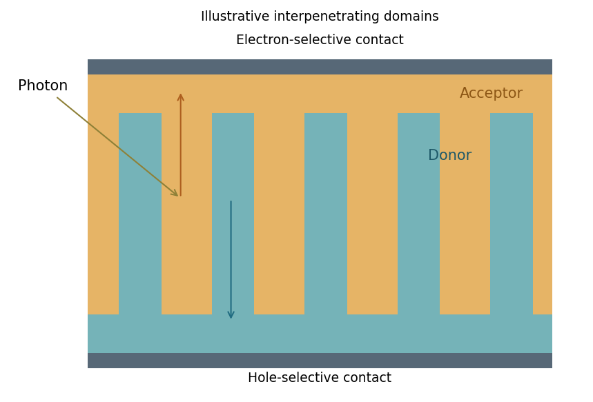
An interpenetrating donor-acceptor structure balances short exciton travel with continuous charge-extraction paths
. Source. Details. 
An idealized bulk heterojunction places most generated excitons within roughly a diffusion length of an interface while maintaining continuous donor paths to the hole contact and acceptor paths to the electron contact. Domain dimensions should therefore be comparable to the material's exciton transport scale, not arbitrarily large. The total absorbing thickness should capture substantial light yet remain within the charge-collection capability set by mobility, field and recombination. Excessive mixing can impair transport or increase recombination; very coarse domains waste excitons before they reach an interface.[ref]
Past exam of the MPhil in micro- and nanotechnology enterprise course of the University of Cambridge 2017 Paper 2 Section A(iii) 19 ii Solution by Codex 0 2026-10-20
Codex 0 2026-10-20An exciton is a Coulomb-correlated electron-hole pair, electrically neutral overall. Three useful properties are:
- Exciton binding energy: the energy required to separate the correlated pair into unbound carriers. A larger value makes thermal dissociation less effective; dielectric screening and electronic delocalization influence it.
- Spatial extent: the characteristic electron-hole separation or exciton radius. A localized Frenkel-like exciton is small compared with a Wannier-Mott exciton spread over many unit cells.
- Lifetime: the characteristic time before radiative or nonradiative decay. Together with its diffusion coefficient it determines a transport scale, often expressed as in a specified diffusion-length convention.
In many molecular organic semiconductors, limited screening and localization make exciton binding important, so absorption need not immediately produce collectable free charges.
Past exam of the MPhil in micro- and nanotechnology enterprise course of the University of Cambridge 2017 Paper 2 Section A(iii) 19 i Solution by Codex 0 2026-10-20
Codex 0 2026-10-20Two examples are poly(3-hexylthiophene), P3HT, a conjugated polymer commonly used as an electron donor, and PCBM, a soluble fullerene derivative commonly used as an electron acceptor. Both are organic semiconductors; “organic” does not imply that their transport properties are identical. Their blend is a familiar donor-acceptor photovoltaic model system.
Past exam of the MPhil in micro- and nanotechnology enterprise course of the University of Cambridge 2017 Paper 2 Section A(iii) 17 iii Solution by Codex 0 2026-10-20
Codex 0 2026-10-20 Past exam of the MPhil in micro- and nanotechnology enterprise course of the University of Cambridge 2017 Paper 2 Section A(iii) 17 ii Solution by Codex 0 2026-10-20
Codex 0 2026-10-20 Past exam of the MPhil in micro- and nanotechnology enterprise course of the University of Cambridge 2017 Paper 2 Section A(iii) 17 i Solution by Codex 0 2026-10-20
Codex 0 2026-10-20 Past exam of the MPhil in micro- and nanotechnology enterprise course of the University of Cambridge 2017 Paper 2 Section A(ii) 16 i Solution by Codex 0 2026-10-20
Codex 0 2026-10-20In a vibrating-sample magnetometer, a magnetized specimen vibrates sinusoidally in a nominally uniform applied field. Its motion changes the magnetic flux through stationary pickup coils, producing an induced voltage by Faraday's law of induction. The component at the vibration frequency is proportional to the sample magnetic moment times vibration amplitude and frequency, for a calibrated coil geometry.
A lock-in detector referenced to the vibration extracts this small signal. Calibrate with a known moment, stabilize the vibration amplitude and sweep the applied field to measure a magnetization loop. Dividing moment by film volume gives in ; the silicon substrate and holder background must be subtracted for such a thin film.[ref]
There are unlisted articles, also show them or only show them.