A transistor whose gate controls an electric field that changes conduction through a channel between source and drain. Changing the gate's electric potential difference controls the channel electric current.
A junction field-effect transistor controls a conducting semiconductor channel using reverse-biased p-n junctions at its gate. Changing gate voltage changes the depletion region and therefore the cross-section available to mobile charge carriers. A depletion-mode n-channel device normally conducts at zero gate-source voltage and is depleted by a more negative gate. The small reverse gate electric current gives high input resistance, while a source-drain supply provides output power.
In an n-channel junction field-effect transistor, increasing drain voltage increases the local gate-channel reverse bias near the drain. The depletion region can meet there, ending the quasi-neutral channel before the drain. Carriers already in the channel are swept across the remaining high-field region, so drain-end pinch-off produces current saturation rather than zero current. A sufficiently negative gate voltage can instead deplete the whole channel and cut the device off. In the one-sided depletion approximation, a channel half-width and donor density give a depletion threshold voltage ; with built-in junction voltage , drain-end pinch-off occurs approximately at .
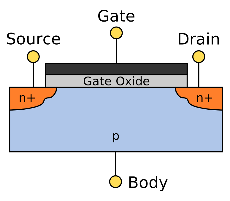
A metal-oxide-semiconductor field-effect transistor, with an insulating layer separating the gate from the semiconductor. Its gate electric field controls the channel's mobile charge carriers; a semiconductor inversion layer can form a two-dimensional electron gas.
An ideal insulating gate blocks particle exchange between the gate and substrate of a MOSFET. Their electrochemical potentials, represented by their band-diagram Fermi levels, therefore need not coincide. An applied gate voltage fixes their difference; with and voltage defined by an electron reservoir, . Contact work-function differences also affect band bending, so equal Fermi levels do not imply flat bands. Each conducting region can separately have a spatially constant equilibrium electrochemical potential.
An integrated circuit technology using complementary MOSFETs. CMOS names a circuit technology; active-pixel sensor names a detector architecture.