An integrated circuit combines interconnected electrical circuit elements in a fabricated structure. A monolithic integrated circuit forms its elements in or on one piece of semiconductor, rather than merely putting separately manufactured components into one enclosure. Transistors supply control in electronic amplifiers; resistors and capacitors can supply bias and timing. Jack St. Clair Kilby's patent describes making such functions from a common semiconductor body with compatible fabrication steps.[ref]
Miniaturized electronic circuits by Jack St. Clair Kilby. Description, opening statement of the invention and discussion preceding Figs. 1–5a
The useful change is to fabricate connections and functions together. Shrinking an enclosure still leaves individual parts to position and join. Integration makes their relative arrangement part of a repeatable fabrication pattern. The distinction is functional as well as geometric: one small piece can implement a whole electrical circuit, while its external terminals expose only the connections needed by its surroundings.
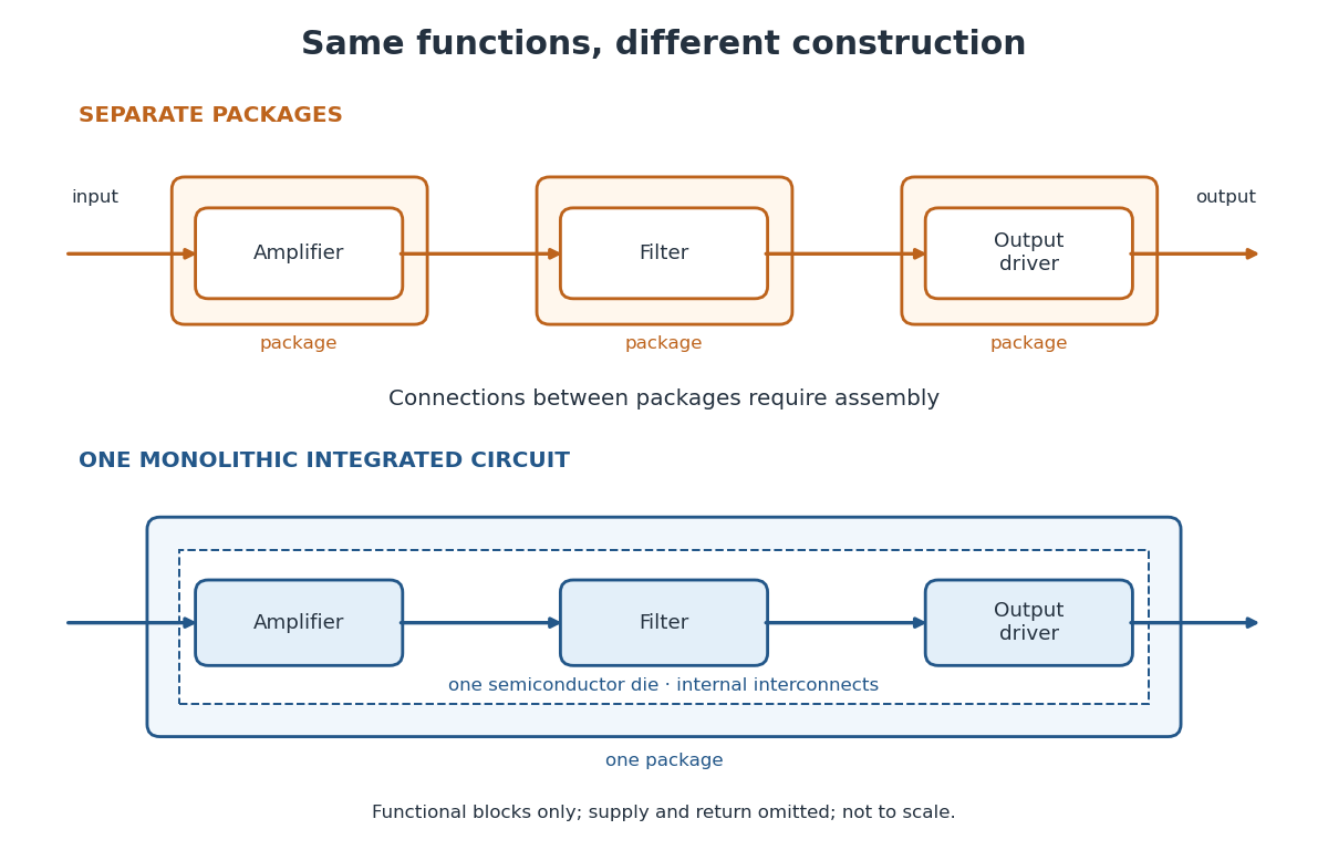
An electrical circuit assembled from separately made components, such as individual transistors, resistors and capacitors. Several functions can share a package without forming a monolithic integrated circuit; packaging alone does not establish how the components were fabricated.
A monolithic integrated circuit has its circuit elements fabricated in or on one semiconductor die. Their connections are essential: an unconnected collection of transistors does not implement the intended electrical circuit.
An original ideal example separates function from fabrication. Connect two resistors, above , in a series circuit across an ideal voltage source. With no load electric current drawn from their meeting point, Ohm's law and the Kirchhoff cycle law giveThese equations apply to either a discrete circuit or an idealized monolithic integrated circuit realizing those same electrical resistances. Integration changes construction; the electrical circuit equations still determine the output. A real load, unwanted capacitance or finite resistor tolerance changes the ideal calculation. Manufacturing many functions together also couples their fate: a fatal defect can discard an entire semiconductor die, motivating the Poisson defect yield model.
In his 2000 lecture, Jack St. Clair Kilby describes an August 1958 comparison circuit made from separate silicon elements. Resistors were cut and etched; capacitors came from diffused, metallized semiconductor wafers. It tested whether semiconductor elements could perform all the required functions, but was still a discrete circuit. For the September prototype he used already diffused germanium material with contacts, cut into bars, and hand-applied wax masks to define a transistor and a distributed resistor-capacitor region. Applying supply power produced an oscillation.[ref]
Turning Potential into Realities: The Invention of the Integrated Circuit (Nobel Lecture) by Jack St. Clair Kilby. Kilby's 2000 Nobel lecture, ChemPhysChem reprint (2001), pp. 486–487, separate-element comparison and oscillator preparation
An inspected eyewitness interview describes the germanium on a microscope slide with protruding wires; changing its connections changed the oscilloscope display from a straight line to a sinusoid. This supplied a qualitative connected/disconnected comparison, not a calibrated record of amplitude, loading or repeatability.[ref]
Oral History of Jay W. Lathrop. Oral History of Jay W. Lathrop, recorded 7 May 2009, p. 11, demonstration and oscilloscope comparison
The inference was feasibility: integrated semiconductor elements could cooperate as an operating electrical circuit. The hand-wired germanium prototype did not yet supply the deposited integrated circuit interconnects of Robert Noyce's silicon design. Nor does a working prototype establish manufacturing yield or long-term reliability.
The planar process fabricates semiconductor devices from a common surface while retaining a protective oxide over the exposed ends of their p-n junctions. Jean Hoerni's patent describes selective openings in silicon dioxide for semiconductor doping and contacts, with oxide left over the p-n junctions. Protection and access are designed together; the surface is not simply stripped after fabrication. This was a distinct enabling contribution to the monolithic integrated circuit.[ref]
Method of manufacturing semiconductor devices by Jean Hoerni. Description, opening problem statement and Figs. 6–10, masking, retained oxide and contact openings
An integrated circuit interconnect is a conducting path joining circuit regions. In Robert Noyce's patent, deposited metal strips cross retained oxide on silicon; selected openings permit contact to the semiconductor while oxide prevents unwanted contact across p-n junctions. Figs. 3–5 combine detection, filtering and electronic amplifier functions using a transistor in one structure. The key is both connectivity and insulation: a metal path must touch its intended terminals while crossing other regions without shorting them.[ref]
Semiconductor device-and-lead structure by Robert Noyce. Description of Figs. 1–5, oxide tongues, metal strips and integrated circuit; claim 1
A thin piece of semiconductor processed to form devices or integrated circuits, often many semiconductor dies together. Dividing wafer area by die area gives an ideal count before edge losses and spaces used to separate semiconductor dies.
A piece of semiconductor carrying a fabricated device or integrated circuit, ordinarily separated from a larger semiconductor wafer. One package can contain multiple semiconductor dies; the package boundary and the semiconductor die boundary are different concepts.
Consider a deliberately simplified model: fatal defects form a spatially uniform Poisson point process with intensity per unit area. A semiconductor die of area works exactly when it contains no fatal defect. Its defect count has a Poisson distribution with expected value , hence its probability of working, called its yield, isThe product is dimensionless. The formula concerns fatal defects, not every visible imperfection. Spatial uniformity, independent defect counts in disjoint areas, and failure from even one fatal defect are model assumptions. Clustering, shared processing failures, repairable regions and defects that affect only some functions can invalidate them. This is a chosen probability model, not historical yield data.
Choose . For semiconductor die areas , and , the model gives , and . Doubling the area squares the yield: . This follows either from the exponential function or by splitting the larger area into two disjoint parts and using independence. More functions on one semiconductor die can save assembly while making the no-defect requirement harder to satisfy.
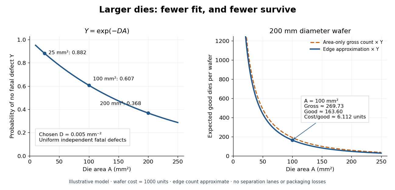
Let a circular semiconductor wafer have diameter and processed cost . For square semiconductor dies of area , ignoring all edge losses gives the ideal gross count . For illustration adopt the geometric edge approximationHere is the good-die count. The correction scales as wafer perimeter divided by die side length: only a boundary strip can lose partially fitting squares. Its coefficient is an approximation depending on layout; the expression is not an exact packing theorem and is useful only when . Counts from it need not be integers. Actual layouts, edge exclusion and separation lanes determine an integer gross count. The expected value of follows by linearity of expectation; independence between semiconductor dies is not required for that step if each has the same yield.
For the original example , , and cost units, and . The predicted good count is per wafer, and the processed cost is units per good die. This is total processed cost divided by expected output, appropriate to a large repeated batch; it is not the expected value of a single-wafer random ratio , which is undefined when . Test, packaging, design and equipment costs are excluded.
A hypothetical test readout makes the inference explicit. Suppose of tested semiconductor dies, each of area , pass a specified functional test. These are invented counts for calculation, not reported measurements. The pass fraction is ; within the Poisson defect yield assumptions it impliesIf pass indicators are independent random variables with common success probability , their sum has a binomial distribution. The fitted standard deviation of the pass fraction is . A test readout estimates pass probability for its tested functions and conditions; it cannot alone establish spatially independent defects, detect every latent failure or distinguish fabrication losses from a faulty test. The logarithm only translates the observed fraction into a defect intensity after those additional assumptions are adopted.
Articles by others on the same topic



It is quite amazing to read through books such as The Supermen: The Story of Seymour Cray by Charles J. Murray (1997), as it makes you notice that earlier CPUs (all before the 70's) were not made with integrated circuits, but rather smaller pieces glued up on PCBs! E.g. the arithmetic logic unit was actually a discrete component at one point.
The reason for this can also be understood quite clearly by reading books such as Robert Noyce: The Man Behind the Microchip by Leslie Berlin (2006). The first integrated circuits were just too small for this. It was initially unimaginable that a CPU would fit in a single chip! Even just having a very small number of components on a chip was already revolutionary and enough to kick-start the industry. Just imagine how much money any level of integration saved in those early days for production, e.g. as opposed to manually soldering point-to-point constructions. Also the reliability, size an weight gains were amazing. In particular for military and spacial applications originally.
Uploaded by the Computer History Museum. There is value in tutorials written by early pioneers of the field, this is pure gold.
Shows:
- photomasks
- silicon ingots and wafer processing