Grow the semiconductor stack epitaxially by molecular beam epitaxy or metalorganic vapor-phase epitaxy on a suitable crystalline GaAs substrate. Sequential changes of source flux or precursor supply set the GaAs/AlGaAs compositions, while dopant supply sets the n-type and p-type regions. Growth time and calibrated rate control the thicknesses of the InGaAs quantum well and the alternating reflector layers.
epitaxy preserves a common crystal orientation and clean, abrupt semiconductor interfaces. These are important both for carrier confinement in the quantum well and for low-loss optical reflection. For a DBR centered at free-space wavelength , the approximate quarter-wave condition is in each layer. Ordinary deposition of a polycrystalline coating would not provide the required active semiconductor heterostructure.
The contact dimensions are readily accessible to UV photolithography followed by directional evaporation and lift-off. A possible sequence is:
- Clean the semiconductor contact surface and coat it with a positive-tone lift-off resist stack. A bilayer giving a small undercut is useful. Soft-bake and align the mask to the intended mesa.
- Use a transparent annular opening in an otherwise opaque mask to expose the contact ring, leaving the central optical aperture covered by resist. Develop away the exposed positive resist. Contact or proximity exposure is adequate for the micrometre-scale ring; projection exposure also works.
- Evaporate the gold contact layer directionally onto the wafer. Keep the resist appreciably thicker than the metal and preserve the undercut so that metal on top of the resist does not bridge continuously to the desired ring. Evaporation is more convenient for lift-off than a strongly conformal coating.
- Dissolve the remaining resist and lift away its overlying metal. The annulus on the exposed semiconductor remains, while the central emitting aperture is free of metal.
A real device must also have appropriate ohmic contact metallurgy. gold alone on arbitrary GaAs is not automatically an ohmic contact: surface preparation, heavy contact-layer doping and, where required, a suitable alloyed contact stack are needed. The schematic gold label specifies the visible electrode, not all such process details. Order the mesa etch and contact steps so that the etchant and any anneal do not damage an already formed contact.
Use a patterned resist or hard mask and anisotropic chlorine-based reactive-ion etching, for example an appropriate inductively coupled plasma process for GaAs/AlGaAs. Ion-assisted removal gives a well-defined mesa with less lateral undercut than an isotropic wet etch. Control etch time or endpoint to obtain the specified approximately depth.
The mask must survive the etch and protect the active aperture. Control ion damage and sidewall roughness, remove residues and passivate the sidewall where required. Compatibility with the metal stack determines whether the mesa is etched before or after front-contact deposition.
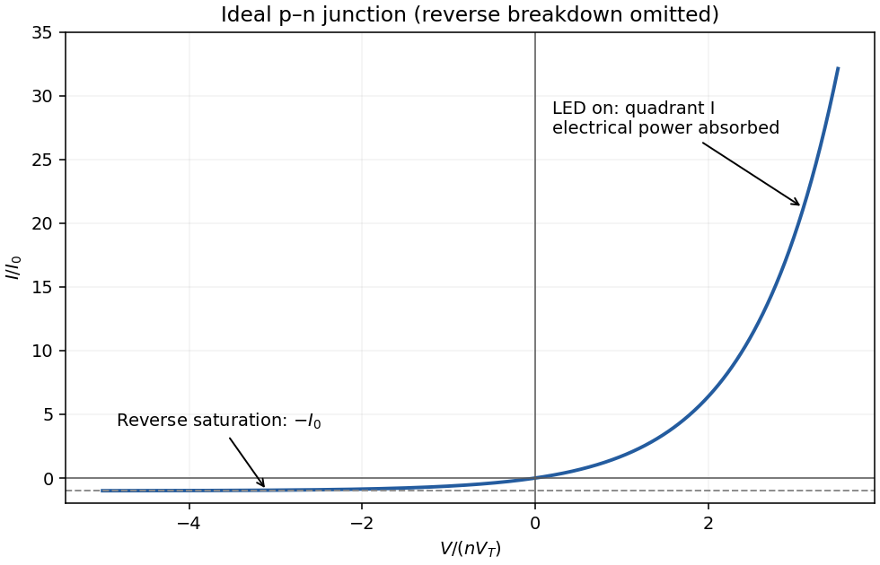
With conventional electric current defined into the positive terminal, an ideal junction hasThe reverse-bias branch tends to before breakdown. In forward bias the electric current rises exponentially; a visibly sharp “turn-on” is a convenient operating description rather than a discontinuity in the equation. A powered LED emits in quadrant I, where , and the device absorbs electrical power . Strong reverse breakdown lies outside the ideal curve below.

forward bias opposes the built-in electric field and lowers the junction barrier from approximately to . In the abrupt-junction depletion approximation,Thus the depletion region narrows and carriers cross the reduced barrier more readily. electron injection into the p side and hole injection into the n side increase strongly, allowing radiative recombination in an LED.
The injected minority-carrier concentrations, and therefore the ideal diffusion electric current, vary approximately as . This produces the steep forward branch of the electric current–voltage curve. One should not extrapolate the depletion-width formula to claim that the junction must lose its entire depletion region before conducting; appreciable electric current flows while a barrier remains, and high injection and series resistance eventually invalidate the simple formulas.
Taking room temperature as , the thermal voltage is . For the stated ideal diode, , soThe term is negligible here. A different precise interpretation of room temperature changes the result noticeably because of the exponential; the calculation above states its temperature explicitly.
For a lower-bandgap material, the intrinsic carrier concentration generally rises, increasing the reverse saturation current density, approximately through with when other parameters are held comparable. Thus the forward electric current at the same voltage would normally increase. If were artificially held fixed at the supplied numerical value, however, the ideal-diode equation would give the same electric current: the band gap dependence enters through the material parameters rather than as a separate term in that equation.
Articles by others on the same topic
There are currently no matching articles.