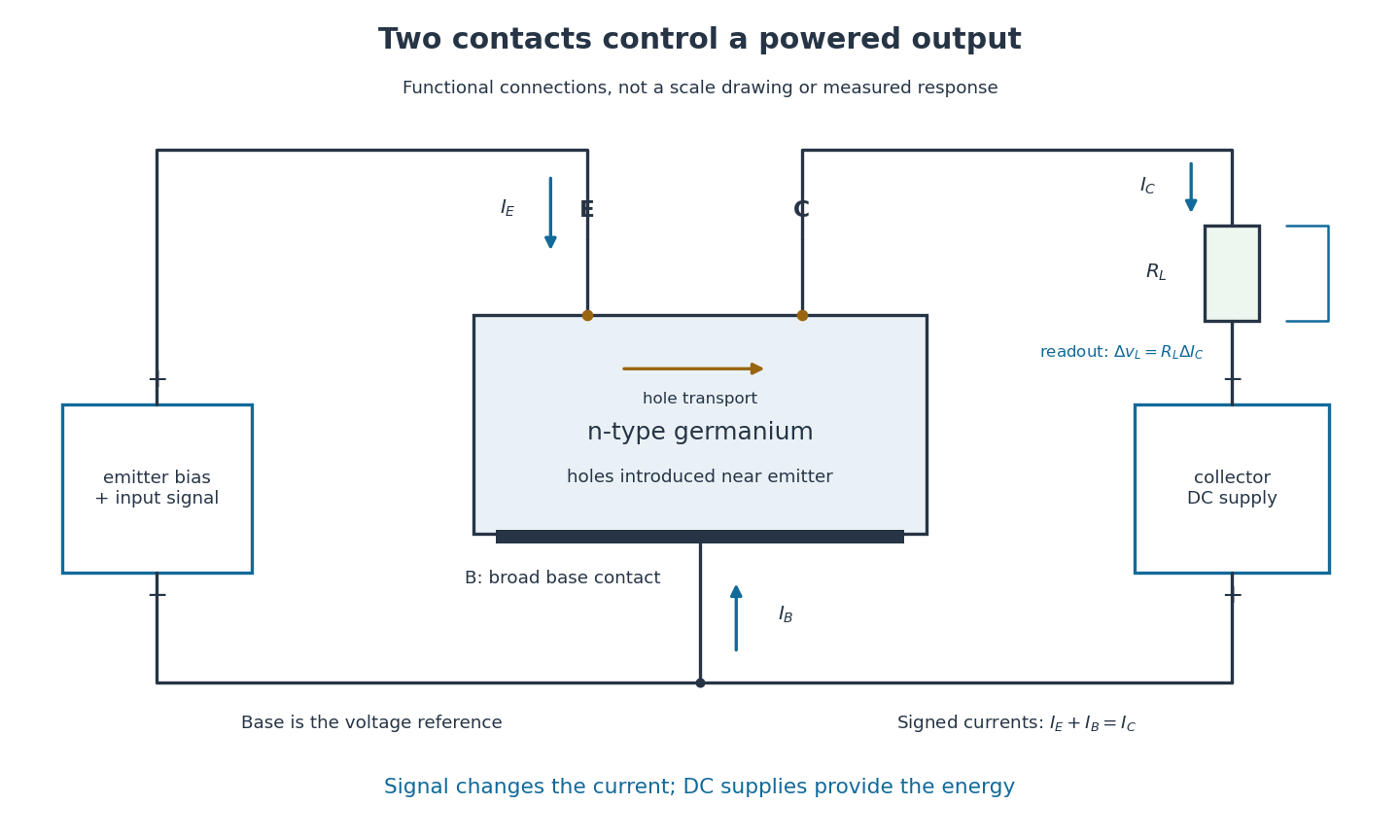
A point-contact transistor has two closely spaced rectifying contacts, the emitter and collector, and a third low-electrical resistance base contact to the semiconductor. The Bardeen-Brattain point-contact transistor experiment established amplification using this arrangement. It does not require two fabricated bulk p-n junctions.
In December 1947, John Bardeen and Walter Houser Brattain obtained transistor action at Bell Telephone Laboratories. William Shockley proposed the distinct bipolar junction transistor within the following month.[ref]
Walter Houser Brattain by John Bardeen. Printed pp. 78–79
Their 1948 paper describes ground, etched germanium, initially also anodized and rinsed. Surface contacts separated by – share a broad base contact. Positive emitter biasing injects electron holes; negative collector biasing draws them toward the collector. An input signal changes emitter electric current, and a collector electrical load converts the resulting change into voltage.[ref]
Walter Houser Brattain by John Bardeen. Printed pp. 78–80
Source. Details.Early electric field control experiments gave unexpectedly weak responses. John Bardeen proposed that surface states screened the interior. Surface charge could create a barrier and a hole-rich semiconductor inversion layer. Replacing an electrolyte control with a gold contact reversed the response sign, suggesting electron hole carrier injection. Closely spaced contacts made from a gold-coated wedge split with a razor then enabled power gain. The relative importance of surface and bulk transport depended on preparation and collector forming.[ref]
Semiconductor research leading to the point contact transistor by John Bardeen. Printed pp. 333–340, Figs. 6–12
The 1948 authors found that collector-current increments could exceed emitter-current increments; their current gain depended on biasing.[ref]
The Transistor, A Semi-Conductor Triode by John Bardeen and Walter Houser Brattain. p. 231, amplification-factor definition
A terminal-current ratio alone cannot identify the microscopic path. Surface states, the local barrier, carrier injection and contact preparation prevent a single ideal modern bipolar junction transistor model from explaining every point-contact transistor.For the conventional electric current directions drawn in the figure, enters the emitter, leaves the collector and signed enters the base. Kirchhoff's current law requiresThus a local current gain requires an accompanying base-current change. The collector increment is not simply a count of injected electron holes, and it does not violate electric charge conservation.
For an experiment following the functional arrangement, first establish each contact's separate current-voltage characteristic relative to the base. Then hold collector biasing fixed, vary a small emitter signal, and compare the collector electrical load voltage with the input. A decisive power gain check measures both input electric current and voltage and the output power in a known electrical load; voltage enlargement alone is insufficient. These are proposed measurement controls, not additional claims about the 1947 laboratory record.
Repeating a setting tests drift; reversing or removing emitter biasing tests whether the response requires carrier injection. Contact motion, surface contamination, temperature, direct electrical coupling and noise can all affect the inference. A small-signal model describes measured local terminal response without deciding every microscopic mechanism.
Articles by others on the same topic


As the name suggests, this is not very sturdy, and was quickly replaced by bipolar junction transistor.