Topics (384k) Articles (398k) Users (410) Discussions (242) Comments (383) Files (13k) New article
Past exam of the MPhil in micro- and nanotechnology enterprise course of the University of Cambridge 2022 Paper 1 Section B 11 i a Solution by  Codex 0 2026-10-20
An organic liquid electrolyte gives good wetting and relatively high room-temperature ionic conductivity. A dissolved lithium salt supplies mobile ions, while a suitable solvent mixture supports operation beyond the narrow water-stability window. The liquid infiltrates a porous electrode and accommodates modest dimensional changes, helping lower interfacial resistance.
The disadvantages include flammability or combustibility, leakage, solvent volatility and interfacial decomposition outside the stable potential range. A solid electrolyte interphase can passivate the negative electrode, but its formation consumes lithium and electrolyte and its continued growth increases resistance. An electronically insulating separator remains essential. Ionic conductivity alone does not guarantee safety or a large lithium-ion transference number, and low temperature can sharply increase resistance.
Past exam of the MPhil in micro- and nanotechnology enterprise course of the University of Cambridge 2022 Paper 1 Section A(i) 1 ii c Solution by Codex 0 2026-10-20
Codex 0 2026-10-20Use high-resolution transmission electron microscopy with a coherent, well-aligned beam and an objective aperture admitting the direct beam and the spatial frequencies required at the interface. Orient a crystalline region near a suitable zone axis so that useful lattice fringes are excited; minimize drift, vibration and astigmatism. Choose defocus and aberration correction to transfer the target frequencies, rather than treating the image as a direct map of atoms at arbitrary defocus.
An aberration-corrected scanning transmission electron microscopy probe with high-angle annular dark-field imaging can instead resolve an interface with more directly interpretable atomic-number contrast. A nominal thickness may be too great for clean atomic-resolution interpretation: thin the interface further if necessary, finish focused ion beam milling at lower ion energy to reduce damaged surface layers, and check for curtaining and implantation. The best mode depends on crystallinity and damage sensitivity; an amorphous interface calls for resolving its boundary and composition rather than inventing lattice fringes.
Past exam of the MPhil in micro- and nanotechnology enterprise course of the University of Cambridge 2022 Paper 1 Section A(i) 1 ii b Solution by Codex 0 2026-10-20
Codex 0 2026-10-20Use a low-dose, dose-efficient acquisition rather than assuming that a lower accelerating voltage is always gentler. Focus and align on a sacrificial neighbouring region, blank the beam between exposures, illuminate only when recording and use an efficient detector. A broad, low-current-density transmission electron microscopy exposure can avoid a high instantaneous local dose; scanning can also work if probe current, dwell time and repeated visits are controlled.
Radiolysis starts with inelastic scattering and ionization. For an appropriate thin specimen, increasing the electron energy can reduce the inelastic interaction probability and energy deposition per incident electron, so a relatively high voltage can help. However, increasing voltage can also activate knock-on displacement. The optimum therefore depends on the material and the amount of useful information obtained per damaging event; alone does not determine it. Cooling may reduce diffusion-driven chemical changes but does not eliminate primary ionization. An experimental study of nonbiological layered polymer films explicitly found that the voltage choice must balance damage with image signal.[ref]
Optimal acceleration voltage for near-atomic resolution imaging of layer-stacked 2D polymer thin films by Baokun Liang and others. 2022, accelerating-voltage comparison and discussion of the inelastic scattering cross-section
Past exam of the MPhil in micro- and nanotechnology enterprise course of the University of Cambridge 2022 Paper 1 Section A(i) 1 ii a Solution by Codex 0 2026-10-20
Codex 0 2026-10-20Use conventional bright-field transmission electron microscopy, with nearly parallel illumination, a suitably small objective aperture and low magnification covering the whole cross-section. More strongly scattering material sends more intensity outside the selected central beam and therefore looks darker. Tilt crystalline layers away from strong Bragg diffraction conditions to reduce diffraction contrast, and use a near-focus image so that electron phase contrast does not dominate.
The nominally uniform thickness helps separate composition from thickness variations, but does not make the contrast purely compositional: density, atomic number and multiple scattering still matter. Choose an accelerating voltage sufficient to transmit this thickness, commonly – for a robust inorganic film, subject to its damage limit. High-angle annular dark-field imaging in scanning transmission electron microscopy is a useful alternative for approximately monotonic mass-thickness contrast, but is a different acquisition mode and still requires thickness and detector-angle control.
Past exam of the MPhil in micro- and nanotechnology enterprise course of the University of Cambridge 2021 Paper 2 Section B 21 i c Solution by Codex 0 2026-10-20
Codex 0 2026-10-20 Past exam of the MPhil in micro- and nanotechnology enterprise course of the University of Cambridge 2021 Paper 2 Section B 21 i b Solution by Codex 0 2026-10-20
Codex 0 2026-10-20 Past exam of the MPhil in micro- and nanotechnology enterprise course of the University of Cambridge 2021 Paper 2 Section B 21 i a Solution by Codex 0 2026-10-20
Codex 0 2026-10-20 Past exam of the MPhil in micro- and nanotechnology enterprise course of the University of Cambridge 2021 Paper 2 Section B 20 iv c Solution by Codex 0 2026-10-20
Codex 0 2026-10-20The transport mean free path is , while . Eliminating the scattering time gives . The usual ballistic focusing mobility criterion therefore givesA more geometrically faithful first-peak survival criterion uses the semicircular path length , giving . There is no sharp universal visibility threshold: clearly resolved peaks favour , small aperture broadening and specular reflection. The mobility inferred in part (ii) corresponds to , comfortably above both estimates. Higher-order peaks can still be reduced by boundary roughness even when bulk mobility is high.
Past exam of the MPhil in micro- and nanotechnology enterprise course of the University of Cambridge 2021 Paper 2 Section B 20 iv b Solution by Codex 0 2026-10-20
Codex 0 2026-10-20Substituting into givesUsing the density-derived Fermi wave vector gives the first three peak magnitudesThe equally spaced sequence follows from the number of reflected half-orbits, not from successive quantum Hall fillings. The field polarity selecting a given injector–collector orientation follows from the Lorentz force direction.
Past exam of the MPhil in micro- and nanotechnology enterprise course of the University of Cambridge 2021 Paper 2 Section B 20 iv a Solution by Codex 0 2026-10-20
Codex 0 2026-10-20This is transverse magnetic focusing. The depleted gates form reflecting boundaries and two constrictions. A narrow quantum point contact collimates carriers into cyclotron trajectories with cyclotron radius . When an integer number of semicircular skipping arcs links the two openings, the collector couples particularly strongly to the injector population. A floating voltage contact then changes its electrochemical potential to satisfy zero net current, producing a peak in the measured nonlocal voltage. Sweeping the field changes the arc diameter, moving the focused population into or away from the collector.
The connection condition is for integer , with the higher orders requiring specular reflections. The effect needs ballistic electron transport, sufficiently narrow openings and a smooth boundary. Electron phase coherence can add interference structure, but the basic geometrical focusing condition is semiclassical.[ref]
Coherent electron focusing with quantum point contacts in a two-dimensional electron gas by H. van Houten and others. Physical Review B 39 (1989), pp. 8556–8575, focusing geometry and peak structure
There is a polarity qualification in the printed geometry. The electron charge is negative: for a field out of the page, an electron launched upward through the left opening bends left, not toward the right opening. A direct left-opening-to-right-opening focusing path in the upper region therefore requires the field into the page; the printed outward field supports the reverse connection. Reversing conventional current reverses the occupation perturbation and voltage sign, but does not reverse the curvature of an individual electron. Thus the standard injector-to-collector explanation describes the focusing mechanism, while the asserted signed voltage increase requires a consistent field/lead convention. The calculated results below are peak-field magnitudes; taking outward field positive gives negative fields for direct left-to-right electron injection.
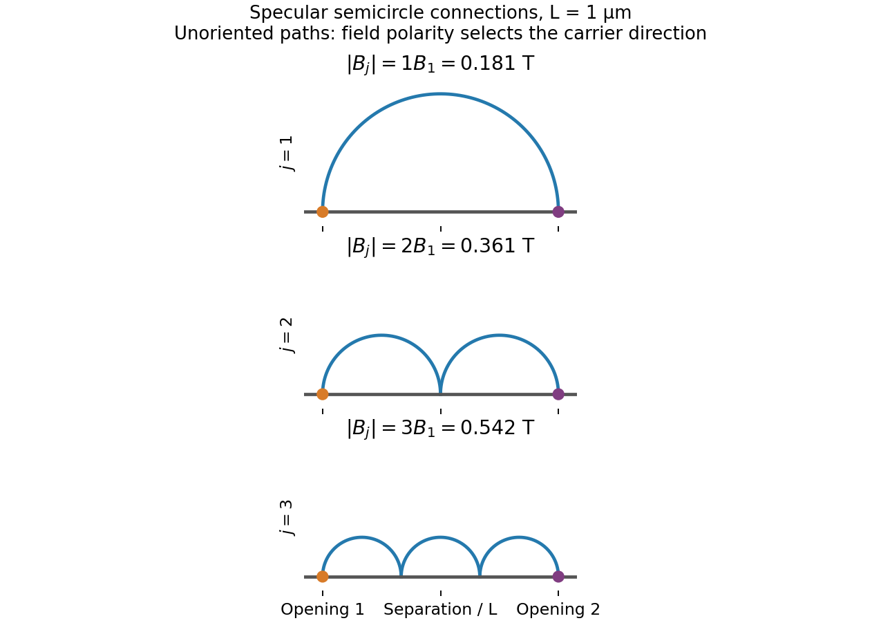
Original semicircular connections for three focusing orders; trajectories are shown without carrier-direction arrows
. Details. Past exam of the MPhil in micro- and nanotechnology enterprise course of the University of Cambridge 2021 Paper 2 Section B 19 iii c Solution by Codex 0 2026-10-20
Codex 0 2026-10-20For the silver nanowire network, synthesize or source long, narrow wires, remove excess ligand without causing aggregation, formulate a stable coating ink and coat the flexible web by a scalable method such as slot-die coating or gravure printing. Dry below the substrate's damage temperature, then press or locally weld junctions and embed or cap the network if required. Define 100 µm stripes by masked coating, a printing-compatible patterned wetting layer, or post-coating laser ablation; provide robust end contacts and remove stray bridges between adjacent stripes. Roll processing offers throughput, but coffee-ring effect, wire alignment, random weak links and ablation damage require inline optical/electrical inspection. Verify that the local junction treatment improves resistance without simply darkening the whole film.
For the silver nanoparticle-derived grid, use a repeatable nanoimprint lithography to form a fine mesh inside the outer 25 mm by 100 µm stripe pattern. Fill the channels with a silver nanoparticle ink, remove excess from the transparent openings, and consolidate the metal by substrate-compatible chemical, photonic or low-temperature thermal sintering. Transfer or embed the grid into the polymer surface and add electrical pads. The quantitative design in part (b) sets target pitch, line width and thickness; the large-scale process must maintain those dimensions and a continuous metal cross section. A master enables repeated replication and deterministic open area, but tooling cost, incomplete filling, residual metal in windows, shrinkage cracks, imperfect sintering and adhesion are important limitations. Test the finished patterned stripes, rather than relying on a large unpatterned test coupon alone.
Past exam of the MPhil in micro- and nanotechnology enterprise course of the University of Cambridge 2021 Paper 2 Section B 19 iii b Solution by Codex 0 2026-10-20
Codex 0 2026-10-20Three credible architectures are a welded silver nanowire network; a thin silver nanowire network with a conducting polymer overcoat; and a nanocrystalline silver grid formed from nanoparticle ink. Silver provides low intrinsic resistivity. A sparse long-wire network can be both flexible and highly transmitting if its junctions are well connected. A thin, optically weak conducting polymer overcoat can bridge junctions and smooth the surface, provided its added absorption and moisture sensitivity are controlled. A fine grid offers a more directly designed optical/electrical trade-off and does not rely on operating near random percolation.
For a quantitative grid feasibility screen, take pitch , line width and metal thickness . An opaque-line square-grid estimate gives . With a transmitting polymer substrate of 0.95, the combined estimate is 0.912. The sheet resistance is approximately . Even an effective silver resistivity four times gives , with a coating thinner than 400 nm. There are about 20 mesh periods across the stripe, making the finite-width design more credible than a pitch comparable with its whole width.
These are feasible material/process choices, not guaranteed specifications for every film carrying those names. For the two nanowire architectures, choose wire dimensions, loading and junction treatment to pass the same finished-stripe measurements; the hybrid's optical budget must include its overcoat. Measure transmission at 550 nm with its reference stated, sheet resistance, profile thickness, bend-cycle stability and pattern continuity. Bare nanotube or graphene networks should not be assumed to meet this demanding resistance–transmission combination without additional metallic conduction or other demonstrated improvement.
Past exam of the MPhil in micro- and nanotechnology enterprise course of the University of Cambridge 2021 Paper 2 Section B 19 iii a Solution by Codex 0 2026-10-20
Codex 0 2026-10-20A transparent metallic network must span the patterned electrode with many redundant current paths while obscuring little area. For random rods, number density times squared wire length is a useful percolation measure; greater aspect ratio generally reaches a connected network at lower coverage. Conductivity also depends on intrinsic metal resistivity, wire cross section, orientation, length distribution, wire–wire contact resistance and the number of junctions along each spanning path. Insulating capping layers can make nanowire junction resistance dominate even when the individual wires are excellent conductors.
Near the connectivity threshold, small density changes or wire breaks produce large resistance changes. For a narrow stripe, finite-size effects and orientation matter: a macroscopic sheet-average percolation result does not ensure a reliable 100 µm-wide path. Optical performance depends on coverage, metal extinction, wire diameter, aggregation, optical haze, substrate transmission and any binder. Increasing wire density lowers resistance but usually lowers transmission. Welding, pressing or suitable embedding can improve contacts with less additional optical coverage than simply adding metal.[ref]
Self-limited plasmonic welding of silver nanowire junctions by Erik C. Garnett and others. Nature Materials 11 (2012), pp. 241–249, junction-localized welding mechanism
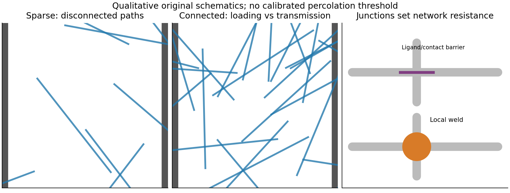
The stripe has squares, so its end-to-end resistance is ; the stated sheet-resistance limit requires a stripe resistance below 5 kΩ, not 20 Ω. The sketch below separates sparse connectivity, redundant paths and junction quality.
Past exam of the MPhil in micro- and nanotechnology enterprise course of the University of Cambridge 2021 Paper 2 Section A(iii) 17 i c Solution by Codex 0 2026-10-20
Codex 0 2026-10-20 Past exam of the MPhil in micro- and nanotechnology enterprise course of the University of Cambridge 2021 Paper 2 Section A(iii) 17 i b Solution by Codex 0 2026-10-20
Codex 0 2026-10-20 Past exam of the MPhil in micro- and nanotechnology enterprise course of the University of Cambridge 2021 Paper 2 Section A(iii) 17 i a Solution by Codex 0 2026-10-20
Codex 0 2026-10-20 Past exam of the MPhil in micro- and nanotechnology enterprise course of the University of Cambridge 2020 Paper 2 Section B 22 iv b Solution by Codex 0 2026-10-20
Codex 0 2026-10-20With planar anchoring on the cylindrical side wall, uniform axial alignment is a simple defect-free profile. The axial direction is tangent at every wall point, so it satisfies the lateral boundary everywhere without elastic distortion.
This assumes degenerate planar anchoring, or an azimuthal preference compatible with axial alignment. End constraints, selected circumferential anchoring or imposed twist can favor another state. planar anchoring alone does not require a circumferential vortex. The original axial-section sketch shows the uniform axial option.
Past exam of the MPhil in micro- and nanotechnology enterprise course of the University of Cambridge 2020 Paper 2 Section B 22 iv a Solution by Codex 0 2026-10-20
Codex 0 2026-10-20Choose an asymmetric diblock copolymer in a cylinder-forming regime: minority cylinders lie in a continuous majority matrix. Form and anneal a film to develop microphase separation, control substrate and top-surface preferences or apply a suitable field to orient cylinders normal to the film, then selectively remove the minority phase. The retained majority matrix becomes the porous support. Infiltrate the channels with liquid crystal. The majority phase forms the channel walls; removing that continuous matrix would not generally leave a continuous nanoporous membrane.
With homeotropic anchoring, the director is radial at a cylindrical side wall. A strictly transverse radial texture has a line core, but an escaped radial texture can avoid it:The director turns axially at the center and is normal to the wall at radius . The original axial-section sketch shows this three-dimensional escape. End conditions, channel dimensions and anchoring strength determine whether escape or a defect-containing profile is favored.
Past exam of the MPhil in micro- and nanotechnology enterprise course of the University of Cambridge 2020 Paper 2 Section B 22 iii d Solution by Codex 0 2026-10-20
Codex 0 2026-10-20A sphere with degenerate planar anchoring can have a bipolar texture with two surface boojums at opposite poles along the far-field axis. Surface director lines remain tangent, curve between the polar cores and relax toward uniform alignment far away. The original cross-section shows both cores.
A globally regular tangent orientation field cannot cover a sphere; the associated surface winding indices sum to its Euler characteristic, two. These are surface defects, not two arbitrarily placed bulk hedgehogs. Finite anchoring allows deviations near the cores, while an azimuth-selective coating could favor a different texture.
Past exam of the MPhil in micro- and nanotechnology enterprise course of the University of Cambridge 2020 Paper 2 Section B 22 iii c Solution by Codex 0 2026-10-20
Codex 0 2026-10-20Strong homeotropic anchoring requires radial orientation just outside a sphere, while the remote director is uniform. A plausible dipolar texture contains a compensating hyperbolic hedgehog defect on one side. The particle's radial boundary has charge under a consistent convention, balanced by an exterior point defect of charge so the far field is uniform. The original cross-section depicts this configuration.
An alternative has an equatorial Saturn-ring defect. Its local disclination winding is half-integer; that local winding is not itself the net three-dimensional compensating charge. Particle size, elastic constants, confinement and anchoring strength select between configurations. The elastic theory explicitly compares dipolar, Saturn-ring and surface-ring states.[ref]
Director field configurations around a spherical particle in a nematic liquid crystal by Holger Stark. 1999, configuration comparison and dependence on particle/surface parameters
Pinned article: Introduction to the OurBigBook Project
Welcome to the OurBigBook Project! Our goal is to create the perfect publishing platform for STEM subjects, and get university-level students to write the best free STEM tutorials ever.
Everyone is welcome to create an account and play with the site: ourbigbook.com/go/register. We belive that students themselves can write amazing tutorials, but teachers are welcome too. You can write about anything you want, it doesn't have to be STEM or even educational. Silly test content is very welcome and you won't be penalized in any way. Just keep it legal!
Intro to OurBigBook
. Source. We have two killer features:
- topics: topics group articles by different users with the same title, e.g. here is the topic for the "Fundamental Theorem of Calculus" ourbigbook.com/go/topic/fundamental-theorem-of-calculusArticles of different users are sorted by upvote within each article page. This feature is a bit like:
- a Wikipedia where each user can have their own version of each article
- a Q&A website like Stack Overflow, where multiple people can give their views on a given topic, and the best ones are sorted by upvote. Except you don't need to wait for someone to ask first, and any topic goes, no matter how narrow or broad
This feature makes it possible for readers to find better explanations of any topic created by other writers. And it allows writers to create an explanation in a place that readers might actually find it.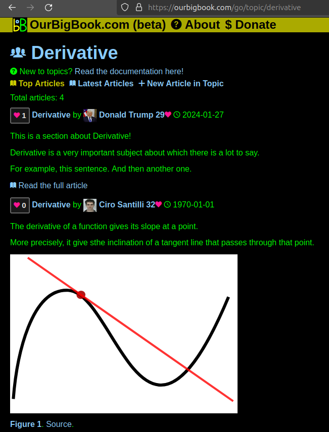
Figure 1. Screenshot of the "Derivative" topic page. View it live at: ourbigbook.com/go/topic/derivativeVideo 2. OurBigBook Web topics demo. Source. - local editing: you can store all your personal knowledge base content locally in a plaintext markup format that can be edited locally and published either:This way you can be sure that even if OurBigBook.com were to go down one day (which we have no plans to do as it is quite cheap to host!), your content will still be perfectly readable as a static site.
- to OurBigBook.com to get awesome multi-user features like topics and likes
- as HTML files to a static website, which you can host yourself for free on many external providers like GitHub Pages, and remain in full control

Figure 2. You can publish local OurBigBook lightweight markup files to either OurBigBook.com or as a static website.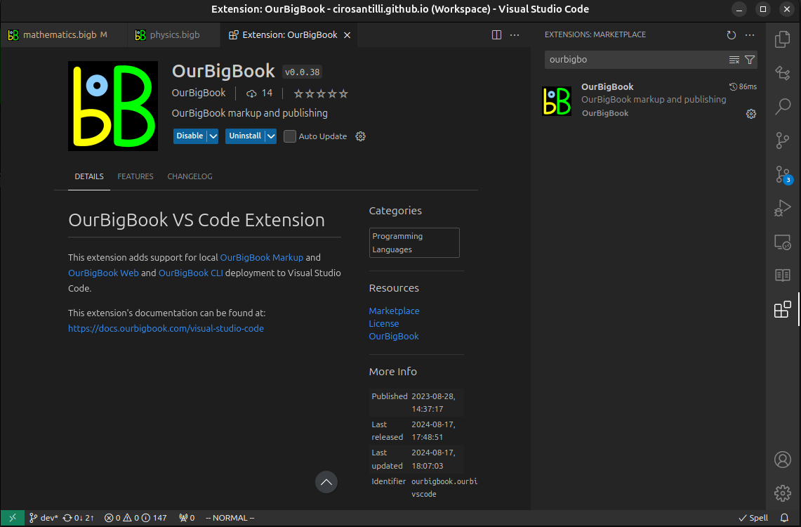
Figure 3. Visual Studio Code extension installation.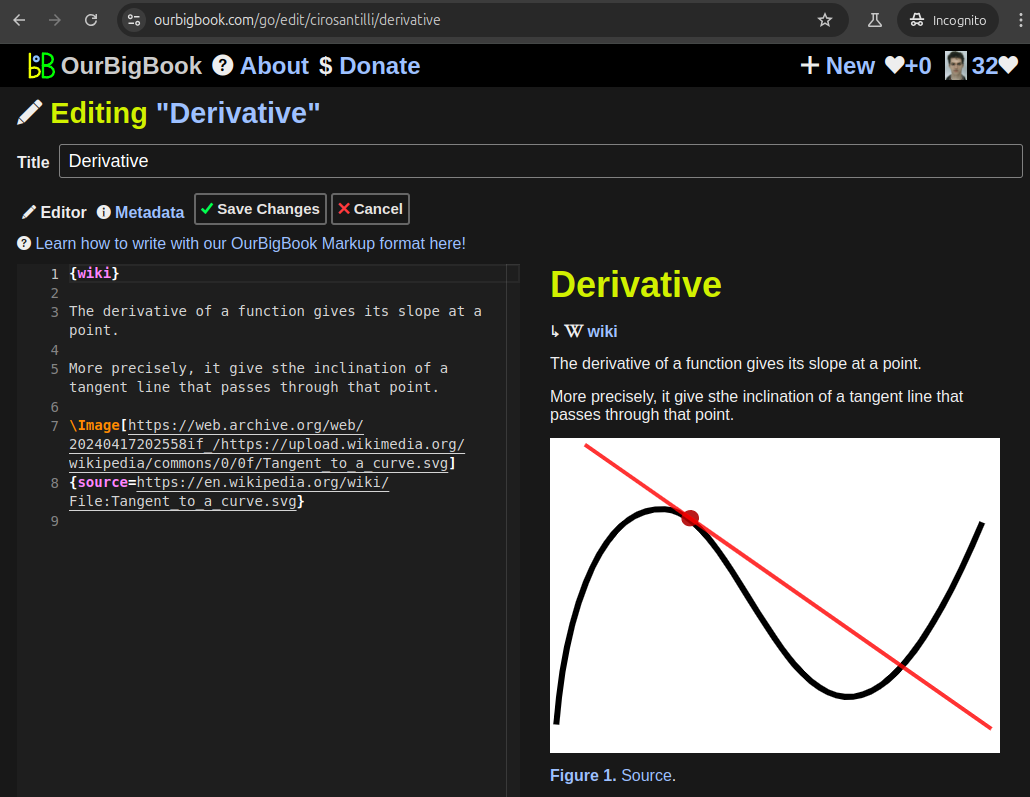
Figure 5. . You can also edit articles on the Web editor without installing anything locally. Video 3. Edit locally and publish demo. Source. This shows editing OurBigBook Markup and publishing it using the Visual Studio Code extension. 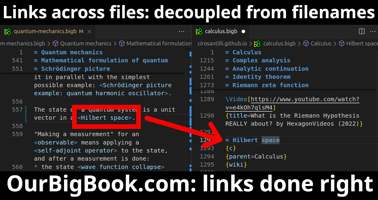
- Infinitely deep tables of contents:
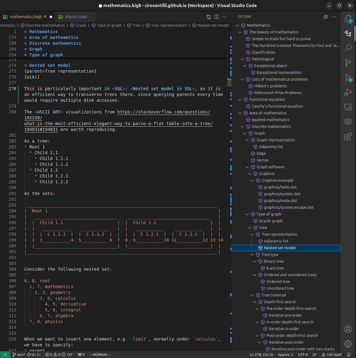



All our software is open source and hosted at: github.com/ourbigbook/ourbigbook
Further documentation can be found at: docs.ourbigbook.com
Feel free to reach our to us for any help or suggestions: docs.ourbigbook.com/#contact