For an intrinsic, nondegenerate semiconductor, charge neutrality and the Boltzmann approximation to the Fermi-Dirac distribution give . Assume the two polymorphs have equal effective-density-of-states prefactors and retain the quoted band gaps at the temperature being estimated. Their carrier-density ratio is thenwith expressed in eV per kelvin. At ,Both absolute intrinsic densities are extremely small at this temperature; a large ratio does not imply that either material is a good intrinsic conductor. Defects or unintended dopants can dominate real “undoped” specimens.
Using the same intrinsic-carrier approximation at givesSimilar mass density and coordination do not prove equal electron and hole effective masses; this result isolates the exponential band-gap effect.
At , the same approximation givesAs temperature rises, the relative advantage from a fixed gap difference becomes smaller, even while the intrinsic carrier densities of both phases increase.
Suitable substitutional donors include Si on a Ga site and O on an N site. The former replaces a group-III atom with a group-IV atom; the latter replaces a group-V atom with a group-VI atom. Each provides an extra valence electron relative to its host site. Si is a plausible substitutional cation-site dopant, and the compact oxygen atom is compatible with an anion site. Site compatibility matters: merely choosing an element with an extra electron without considering which sublattice it occupies is insufficient.
A standard substitutional acceptor choice is Mg on a Ga site: a group-II atom replaces group III, leaving one fewer valence electron. Its size is sufficiently compatible with the cation sublattice to make substitution plausible. This identifies the intended acceptor chemistry; actual hole density also depends on activation, incomplete ionization and compensation. Size and valence rules alone do not guarantee a shallow, fully ionized acceptor.
At equilibrium, electrons initially diffuse from the n side and holes from the p side. Recombination leaves ionized donors and acceptors in a depletion region, producing an internal electric field and band bending. The Fermi level is constant across the equilibrium p-n junction. With p material on the left, both band edges lie higher on the p side, as in the left panel.
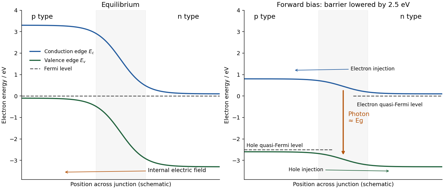
Equilibrium and forward-biased direct-gap p-n junction energy bands, with injection and photon emission
. Details. 
Forward bias, with the p side positive relative to n, reduces the injection barrier. Electrons and holes enter the junction region and can recombine radiatively, emitting photons with energy close to the band gap. Under bias, separate electron and hole quasi-Fermi levels replace a single equilibrium Fermi level.
Both GaN polymorphs have a direct band gap, so a conduction-band electron and valence-band hole can recombine without a large crystal-momentum change. Silicon and germanium have indirect band gaps, requiring phonon assistance for near-edge radiative recombination, which makes efficient band-edge light emission much harder. A direct gap enables the process; defects, carrier confinement and competing nonradiative channels still determine device efficiency.
Using and an ideal band-edge photon energy equal to the quoted gap,At low temperature an electron and hole can form a bound exciton. Its recombination releases approximately , so its wavelength is longer than evaluated using the gap at that same temperature. GaN excitation and emission measurements resolve such excitonic transitions below the fundamental gap.[ref]
Fundamental energy gap of GaN from photoluminescence excitation spectra by Bo Monemar. Photoluminescence-excitation, reflection and emission comparison; separation of exciton transition energy from the fundamental gap
For the quoted cubic-phase gap,The same exciton binding argument can shift the actual emission to longer wavelength; impurity-bound transitions can also lie below the fundamental gap. The comparison must use at the operating temperature. Ordinary temperature-dependent gap changes can shift the band edge in the opposite direction, so the numerical values based on fixed supplied gaps are not universal lower bounds for every cooled device.
GaN has a substantial band-gap advantage for high-temperature operation. Its gap is larger than those of GaAs and GaP, suppressing thermally generated intrinsic carriers through . A doped junction therefore retains its intended carrier imbalance and can have lower thermally generated leakage over a wider temperature range, other factors being equal. The wide gap also supports emission at higher photon energies.
This is a materials-based expectation, not a guarantee for every finished device. Dopant activation and compensation, defects, contact stability, heat extraction and nonradiative recombination can set the practical limit. Increasing temperature also reduces carrier mobility and can broaden or quench light emission. The relevant advantage is reduced intrinsic excitation; a comparison of operating temperatures needs those other device properties too.
Articles by others on the same topic
There are currently no matching articles.