
Take . It has exactly two nonzero entries, both one, but . Thus it is not an idempotent matrix. Its being an orthogonal matrix does not make it an orthogonal projector.
Using the unit length of ,Then ordinary matrix expansion gives . Both and its complementary matrix are projectors. The second calculation in fact holds for every idempotent matrix, without requiring the matrix to equal its transpose.
Consequently for every . Taking successively as the standard basis vectors shows that every column of this difference is zero. Hence . Equality on one selected vector would not suffice; here it holds on all vectors.
For nonzero , let be its angle to the unit vector . The scalar projection on the oriented axis is . Since , the dot product identity gives . Multiplying that signed scalar by places the foot at .
The residual is perpendicular to the axis, because . An obtuse angle gives a negative scalar and a foot on the negative side of the line; has projection zero without needing an angle.
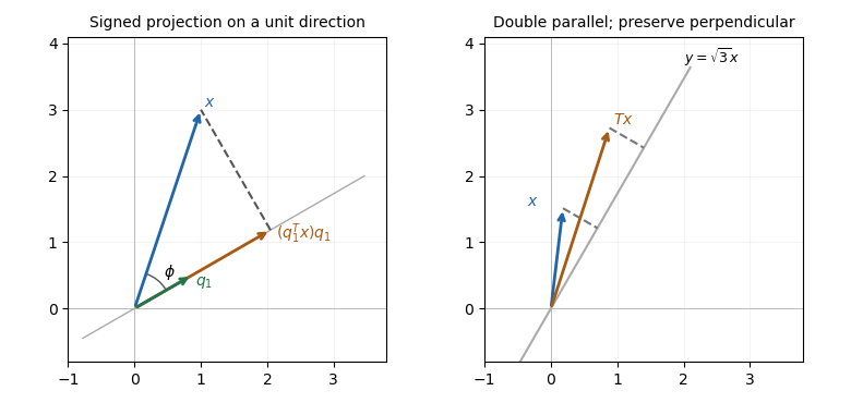
Projection drops a perpendicular to a unit direction; directional stretching doubles only the parallel component
. Details. The first panel is a constructed geometric illustration. The second illustrates the directional stretch used later in Question 6.
The likely effect in a single-cycle or unchanged pipeline-stage implementation is a longer combinational critical path and hence a lower maximum processor clock frequency. Previously the barrel shifter and ALU could work in parallel before result selection; the modified path can require both shift and addition before address or result use.
Ignoring common processor register and wiring delays, the relevant combinational logic contribution changes roughly from to , with any additional input selection included as needed. The processor clock period must also cover processor register timing and the rest of the instruction path, potentially including memory access. Removing a multiplexer offsets some delay, so a numerical frequency change cannot be inferred without component timings. Pipelining, a faster implementation or another pre-existing bottleneck can alter the outcome; the changed serial dependence is the reason for the likely reduction.
A useful additional mode is base plus scaled register indexing, with effective address . For an array of four-byte elements choose , use its base address on the unshifted ALU input and its index processor register on the barrel shifter input, then add. This forms an indexed machine word address in one datapath pass. An eight-byte element uses .
With parallel ALU and barrel shifter outputs, shifting and adding require either separate instructions/cycles or another route from the barrel shifter to the ALU. The new serial connection supplies that route. This is an addressing mode capability, not a claim that the old instruction encoding already contains the new mode.
SP-relative addressing forms an effective memory address by adding an offset to the stack pointer. It accesses local variables, saved processor registers or other stack-frame data without dedicating a separate base processor register for each object. The supplied reference gives word-aligned SP-relative offsets from to , which corresponds to an eight-bit nonnegative field scaled by four.
In the modified datapath, select the stack pointer for the unshifted ALU input, the instruction immediate operand for the barrel shifter input, and ALU addition. The effective address can then be . Scaling the immediate operand changes the reachable displacement range without storing a larger immediate operand. For example, an eight-bit field shifted by two reaches offsets through ; shifting it by four reaches through , but only on a sixteen-byte grid. Larger range and finer address granularity are different properties, so the extra reach is not free arbitrary-byte addressing.
The parallel layout cannot feed a shifted immediate operand directly into its address-producing ALU in the same pass. The serial layout can. The actual immediate operand width and permitted shift encodings of a new instruction must be specified; the question does not fix them, so no particular enlarged instruction encoding is implied.
Use five cascaded banks of 32 two-input multiplexers, for optional shifts of bits. The original circuit schematic below shows one bank per shift-amount bit; this is a left bit shift with zero fill, not a bit rotation.
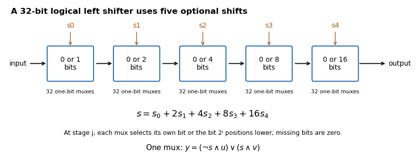
If , stage selects either its unchanged input or that input shifted left by . For bit position , the shifted candidate comes from position when it exists, and otherwise from zero. Composing the chosen stages shifts by the sum of their distances, so each amount from to is represented exactly by its five binary control bits. There are one-bit multiplexers, with five multiplexer delays along a bit path.
The following original schematic shows the two data organisations. Register-address, write-enable and memory controls are common background; the diagram highlights the changed combinational logic paths.
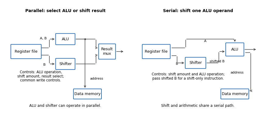


In the parallel design the result-source multiplexer selects either the arithmetic logic unit or barrel shifter. Its control is additional to the ALU function and shift amount. (i) Addition: read the two operands, select ALU addition and select the ALU result; the shift amount is irrelevant. (ii) Constant left bit shift: read the operand to be shifted, set the shift amount from the immediate operand and select the barrel shifter result; the ALU operation is irrelevant.
In the serial design the result comes through the ALU, so that result-source selection disappears. Its shift-amount control is now relevant to arithmetic as well. (i) Addition: set the barrel shifter to zero shift and select ALU addition, so its inputs are the unshifted processor register values. (ii) Constant left bit shift: set the requested shift and select an ALU operation that passes the shifted operand through. If the ALU lacks that operation, implement it or provide a selectable zero on its other input and add zero. This requirement should be stated, rather than assuming that an ordinary two-input add automatically performs a shift alone.
The ALU result can still supply the memory address. For a register-result instruction, enable processor register writeback and leave memory writes disabled. If the ISA requires shift carry flags, the flag-generation control must retain the barrel shifter's outgoing-bit information; blindly using a pass-through ALU's arithmetic carry is insufficient.
Maintain a counter and independent timed finite-state machine for each detector–light pair, while sharing the interrupt scan and timer infrastructure. Blocking for one channel's flash would unnecessarily delay every other channel.
eye_handler():
    for i in all_channels:
        if EYE_DETECTED[i] != 0:
            EYE_DETECTED[i] = 0
            pending[i] = pending[i] + 1

main_event_loop():
    initialise each LIGHT[i] = 0
    initialise pending[i] = 0, state[i] = IDLE
    enable detector interrupts
    forever:
        now = monotonic_timer_snapshot()
        for i in all_channels:
            service_channel(i, now)
        arrange the next wake-up for new work or the earliest deadline
service_channel is the three-state sequencer from (a), with its own started[i] and an interrupt-safe try_take_event(i). Shared interrupt demultiplexing uses separate if tests, not an else if chain: simultaneous pending detectors must all be acknowledged and counted. If a new detector becomes pending during the scan, the controller must retrigger while a flag remains set or the handler must rescan appropriately; the exact interrupt controller semantics must be checked rather than assuming a single scan can never miss an edge.One hardware timer can schedule the earliest active channel deadline. On its expiry, service every due channel and rearm for the next deadline; a periodic tick with adequate resolution is a simpler alternative. Detectors and the timer can then interleave without serial one-second waits. The handler/main-program counter accesses need the same short critical section protection as in (a). Keep timing state in one execution context, or protect it too if both a timer handler and the main program modify it.
The loop invariants are per channel: the pending count equals recorded but unstarted events,
ON means that channel's light is on, and GAP prevents a new flash until one second after its preceding light-off transition. Different channels may flash simultaneously. The event latch rearming limitation, finite backlog capacity and timer-resolution qualifications apply independently to each channel. These cannot be solved by replacing several event counters with one global Boolean variable. There are unlisted articles, also show them or only show them.