Use anisotropic alkaline wet etching of a suitably oriented crystalline silicon wafer. A KOH- or TMAH-based process etches crystallographic planes at different rates, leaving slow-etching facets as a pyramidal texture on a wafer. The facets redirect reflected light towards neighbouring surfaces, increasing the chance of absorption rather than specular escape.
Choose conditions that give a uniform texture without excessive removal or contamination, and clean the wafer before forming the junction. This mechanism depends on crystallinity: a multicrystalline or differently oriented wafer may need another texture process. The drawing alone does not establish the wafer orientation, so the standard pyramidal-texture method carries that explicit assumption.
Diffuse a donor such as phosphorus into the textured p-type surface, then control the thermal drive-in to form the shallow n-type emitter. A phosphorus-containing vapour source can supply the donor over the exposed area. Diffusion and activation create an n-on-p p-n junction; remove the phosphorus-rich surface glass and isolate the rear and wafer edges as required to avoid shunts.
An alternative is ion implantation followed by an activation and damage-repair anneal. The diffusion route is particularly convenient for large-area coverage of a textured wafer. The indicated roughly layer is a depth target for process control, not an instruction to grow an undoped film and assume that it becomes n-type.
Deposit hydrogenated silicon nitride by plasma-enhanced chemical vapor deposition. A plasma activates a silicon-containing precursor and a nitrogen source, enabling a conformal thin film at a lower substrate temperature than a purely thermal process. Tune gas composition, power and time to control thickness, refractive index, stress and hydrogen content.
The film serves as an antireflection coating and can also provide chemical and field-effect surface passivation. As a simple optical check, a quarter-wave thickness is ; and correspond to a design wavelength near . The textured surface and broadband illumination require a fuller optical optimization, so this check is an order-of-magnitude explanation rather than an exact reflectance calculation.
X is an aluminium-doped back surface field region. Annealing alloys the rear aluminium with silicon; on cooling, silicon regrowth adjacent to the contact incorporates aluminium as an acceptor. This creates a more heavily p-type region between the p-type base and rear metal contact.
The resulting doping gradient creates a field that reduces the minority-electron population near the recombination-active rear metal interface. It therefore reduces rear-surface recombination and improves collection of photogenerated carriers. Heavy doping also helps form a low-resistance majority-carrier contact. This is a rear isotype doping transition, not the front n–p junction and not an electrically insulating blocking layer.
In physical vapor deposition, material is physically released from a source and transported to the substrate, where it condenses. Three examples are thermal evaporative deposition, electron-beam evaporation and sputtering. Their angular distributions, source heating and energetic bombardment differ, even though all belong to the physical-deposition family.
In chemical vapor deposition, volatile reactants undergo chemical reactions that produce a solid film at or near the substrate, with gaseous products removed. Examples are atmospheric-pressure thermal CVD, low-pressure CVD and plasma-enhanced chemical vapor deposition. These are three established process variants, distinguished by pressure and activation method. Surface chemistry, precursor delivery and temperature determine growth, rather than condensation alone.
Atomic layer deposition is a related cyclic surface-reaction method, but need not be counted as a separate conventional CVD example to satisfy the requested three. Reactive sputtering can involve chemistry, so the boundary is best explained by the dominant source and transport mechanism rather than by claiming that a PVD chamber can contain no chemical reactions.
Choose conventional diode current as positive in forward bias. The ideal dark and illuminated current densities areThe dark reverse-bias asymptote is before breakdown. Illumination shifts the curve down by : the short-circuit point is , and the open-circuit point is . The power-generating region has positive voltage and negative diode-convention current. A plot using positive delivered current would flip the vertical sign; its physical intercepts are the same.
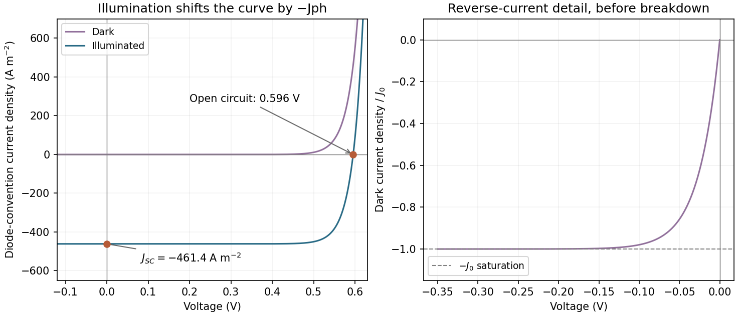

Assume one collected electron per absorbed photon, ideality factor one and . The question does not specify temperature, so the result should also be understood through its temperature-dependent formula. The photocurrent density isAt open circuit the diode current balances that photocurrent:Using gives approximately . These are current densities, so no device area is needed. Incomplete collection would replace by the collected current and reduce this estimate.
Without texturing, more incident photons generally escape by reflection, so the absorbed flux and decrease. Holding and temperature fixed, the voltage falls logarithmically: if absorption is multiplied by and , then . A real texture also changes surface area and recombination, so an unchanged is an assumption rather than a guarantee.
Articles by others on the same topic
There are currently no matching articles.