Count wavevectors in a large volume with periodic boundary conditions. One spin-degenerate spherical band suppliesFor the conduction band, and . Transforming the state count to energy givesFor the valence band use and , obtainingEach density of states is zero beyond its indicated band edge. The factor two counts spin; an extra valley degeneracy was not assumed in these stipulated isotropic bands.
In the nondegenerate conduction band, the Fermi-Dirac distribution reduces to its Boltzmann distribution tail. ThusHere the substitution leaves . For electron holes use the empty-state probability , not the conduction-band Boltzmann factor. This givesThe chemical potential cancels in the product. With ,This semiconductor mass-action law holds in thermal equilibrium for nondegenerate carriers, including a doped semiconductor. Only in an intrinsic semiconductor must . The factors are the effective density of states; the factor in the final expression follows from the two spin factors already included in (a).
Ordinary doped semiconductor devices need a regime where their donor impurities or acceptor impurities supply mobile charge carriers while intrinsic thermal excitation remains sufficiently small.
At low temperature, donor impurities or acceptor impurities may no longer be ionized. Dopant freeze-out reduces the carrier density, raises electrical resistance and changes the intended carrier injection and p-n junction response. At high temperature the intrinsic carrier concentration grows aswhen band effective masses and band gap are treated as constant. Once it becomes comparable with the net doping density, it overwhelms the intended electron-hole imbalance; reverse leakage and dissipation increase and useful p/n control is lost.
The usual operating window lies between freeze-out and intrinsic conduction, with mobility and thermal management placing further practical limits. This is a statement about conventional doped-device operation, not a fundamental prohibition on engineered cryogenic or wide-bandgap devices.
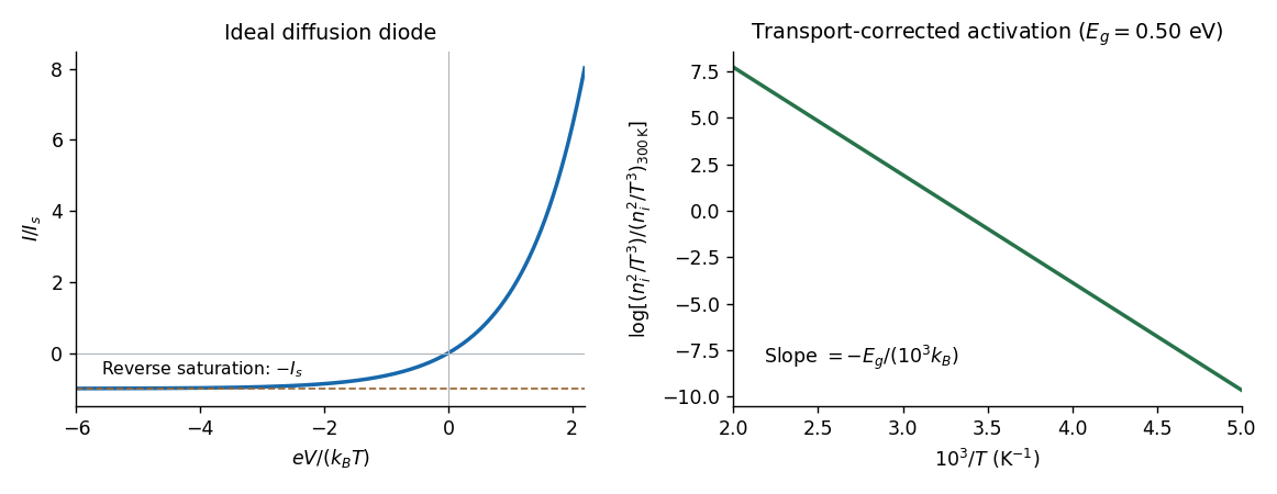
An ideal diffusion-dominated p-n junction obeys the Shockley diode equationwith diode ideality factor in the simplest model. Forward bias gives exponential current growth; reverse bias gives a nearly constant until diode reverse breakdown, outside this ideal expression.
For a long abrupt p-n junction in low carrier injection, the diode saturation current isHere is area, are ionized dopant densities, and are minority-carrier diffusion coefficients and diffusion lengths in the appropriate regions. At each temperature, extract either from the reverse-saturation plateau below breakdown or from a forward exponential fit using its measured diode ideality factor.
Extracting a semiconductor band gap from diode saturation current requires correcting for the transport prefactor:A plot against has slope when the gap and effective masses are nearly temperature-independent. Alternatively divide the measured by a known to recover the full . The prefactor cannot generally be assumed constant over an arbitrarily broad range. Junction-generation or recombination-dominated current can scale as instead, so the diffusion regime should be identified from the current-voltage behaviour.

A current-carrying sample in a transverse magnetic field develops a transverse electric field because the Lorentz force deflects its charge carriers. In steady state this Hall voltage balances the transverse deflection. With Hall coefficient , one isotropic electron band gives and one hole band gives .
When Electrons and electron holes both conduct, the weak-field two-carrier result isThe two-carrier Hall coefficient weights each species by mobility squared. Its sign changes whenTemperature changes dopant ionization, intrinsic electron-hole generation, and the two charge carrier mobilities, so it can move the system across this condition. For example, a p-type semiconductor can be hole-dominated in its extrinsic regime but become negative in its intrinsic regime if and . A sign change is possible, not mandatory: in many n-type semiconductors Electrons dominate at both temperatures. The density majority alone does not determine the Hall sign in a two-carrier material.
Articles by others on the same topic
There are currently no matching articles.