Take as the signed electron charge. The Lorentz oscillator model is a driven damped bound charge:The first term is inertia, the second is a phenomenological frictional loss of coherent motion to other degrees of freedom, and the third is the linear restoring force from binding to the atom. The driving term is the electric force. The natural angular frequency represents the electronic transition; this classical oscillator describes its near-resonant linear response. The friction convention is , so no factor two is hidden in .
Substitute harmonic amplitudes with the specified convention:One electron contributes a dipole moment , so the electric polarization of a density isUsing givesThus the paper's dimensionless is the relative permittivity, rather than the absolute permittivity . The electron's negative charge disappears from the electric susceptibility because both the force and dipole moment contain .
Set . The real part and imaginary part of the complex permittivity areFor positive frequency the loss part is nonnegative. The real part starts at , rises below resonance, falls steeply through the resonance region, and approaches one from below at high frequency. The imaginary part is a positive absorption peak near , tending to zero on both sides.
For a nonmagnetic medium write its complex refractive index as , with and optical extinction coefficient . In a transparent region with and ,The real part controls phase velocity and optical dispersion; the loss part controls wave absorption and the cycle-averaged dissipated power density . Weak damping gives a narrow line but does not make wave absorption weak at its centre. The transparent-medium approximation applies away from the line.
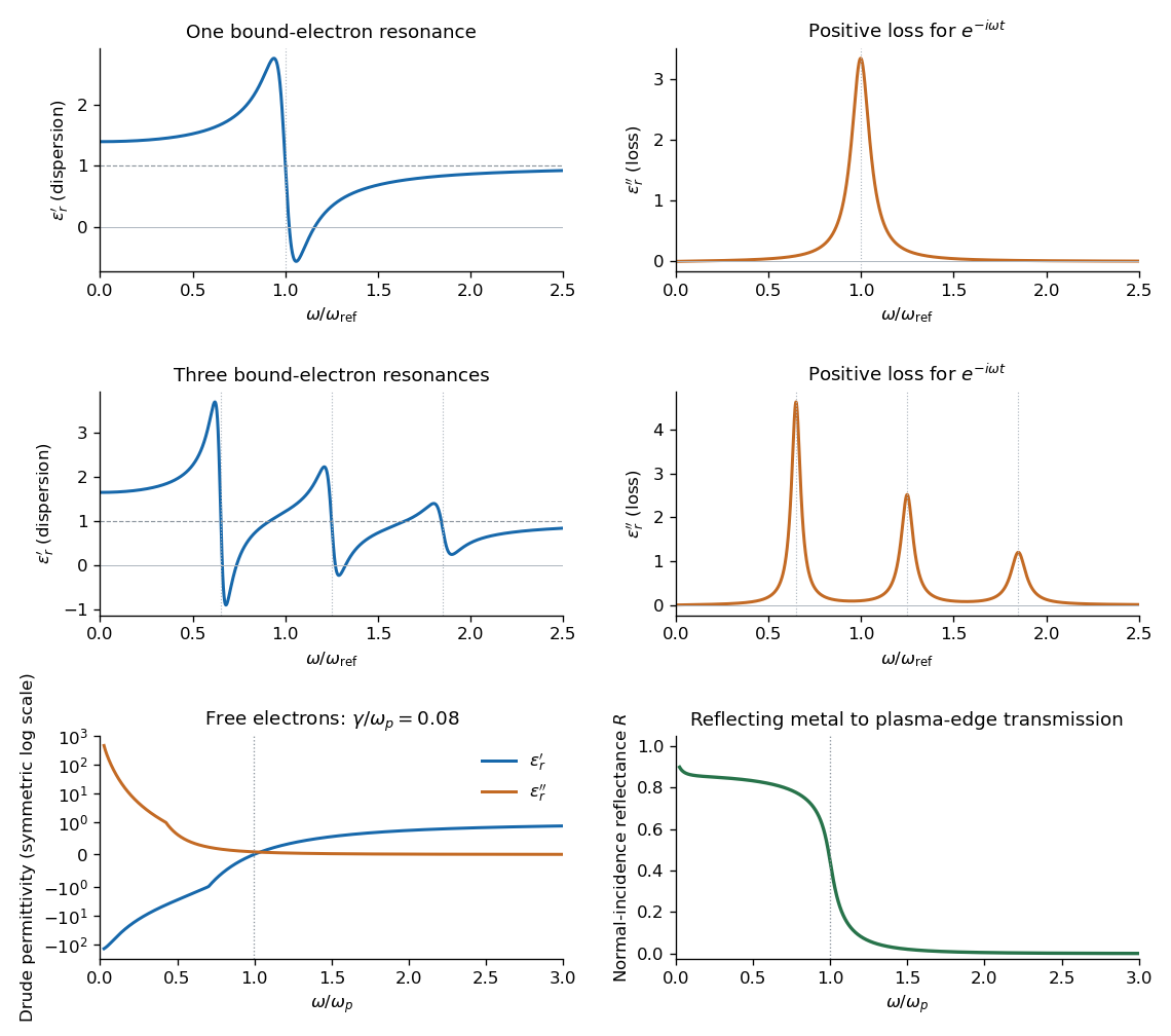

For independent electronic transitions, add the electric dipole moment responses:The positive constants include electron density and transition atomic oscillator strength. Each term adds an absorption peak to and a dispersive positive-to-negative contribution to , as in the middle row of the figure.
Between well-separated absorption lines, where the medium is transparent, the refractive index generally increases with frequency: , or . This is normal dispersion. Near a resonance the real response turns down with increasing frequency, producing an interval of anomalous dispersion, , accompanied by appreciable absorption. The absorptive and dispersive parts are linked by the Kramers-Kronig relations; the steep variation is not independent of the loss spectrum.
An unbound conduction Electron has no local restoring force, so set while retaining inertia and momentum relaxation time . This is the Drude model:Separating the response givesFor a good metal, . The real part is strongly negative at low frequency, crosses zero at , and approaches one from below. The imaginary part diverges as at low frequency, reflecting the finite dc electrical conductivity , then decays as . The low-frequency imaginary response describes conduction loss, not a finite-frequency bound-electron absorption line. Core-electron and interband responses can add a background in a real metal.
At normal incidence from vacuum, the Fresnel equations give the reflectanceA good metal has close to one below its plasma frequency. At very low frequency the electromagnetic field penetrates only a skin depth; the local Drude limit gives . In the collisionless negative-permittivity range the transmitted field is evanescent and reflection remains strong. Near the plasma edge the reflectance drops sharply; above it and propagating waves become possible. In the ideal free-electron high-frequency limit,Finite damping rounds the plasma edge, and interband absorption changes the detailed response of actual metals.
Choose one atomic orbital and on the two atoms and approximate a molecular orbital by the linear combination of atomic orbitalsProjecting the Schrödinger equation onto the two orbitals gives a generalized eigenvalue problem , where and . In an orthonormal basis the matrix isThe coupling mixes the atomic states and produces a lower bonding molecular orbital and upper antibonding molecular orbital. For equivalent real orbitals with overlap the normalized combinations are ; the precise energy ordering follows from the Hamiltonian matrix elements. This restricted orbital basis is an approximation to the molecule's wavefunction, rather than a claim that exact isolated-atom orbitals remain unchanged in the molecule.
A concrete example is samarium hexaboride, : narrow, nearly localized -derived states mix with a much more dispersive -derived conduction band. Such band hybridization is the low-energy mechanism behind a bulk Kondo insulator gap. The two-band Hamiltonian is an effective illustration; correlations help set its narrow-band energy and renormalized mixing.[ref]
https://www.nature.com/articles/ncomms3991. Introduction: nearly localized flat f bands hybridize with a dispersive d-derived conduction band in SmB6
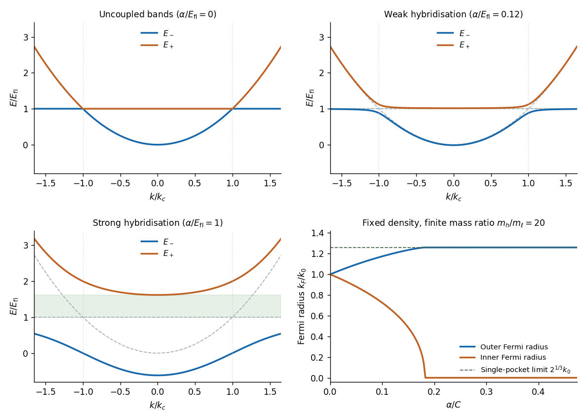
Write the dispersive band as with and define . The uncoupled sketch is an upward-opening parabola and a horizontal flat band at positive energy. They cross on the sphere in three dimensions, or at in a one-dimensional cut:Without mixing the crossing is allowed. The left panel of the figure shows this case.

For dimensional clarity in the usual band effective mass convention. The printed product is consistent only if is a curvature coefficient with inverse-mass units; it cannot simultaneously denote the effective mass itself. Using avoids relying on that notation.
At nonzero band hybridization, the crossing becomes an avoided crossing. The separation at is . If , appreciable mixing occurs only where ; away from that region each branch retains nearly its original orbital character. For , the avoided crossing is broad and both branches are substantially reshaped, as shown in the figure.
Use for the lower branch and for the upper one. For ,The lower branch increases towards from below. Thus an indirect gap exists in the exactly flat-band model. In the unbounded-parabola limit its lower bound isA finite Brillouin zone gives a finite maximum of below and hence a slightly larger indirect gap. This hybridization gap differs from the local direct gap .
The material can therefore be a band insulator when the lower band is full and the upper band empty. With two spin-degenerate orbitals per unit cell, the required filling isWith spin degeneracy removed, replace two by one for each independent spin sector. Other fillings are metallic in this noninteracting model.
At each wavevector the orbital-basis Hamiltonian isA phase choice makes the momentum-independent mixing real and nonnegative. The characteristic equation issoFor , an eigenvector obeys . At the bare crossing, the normalized states are with energies . The lower state's parabolic-orbital weight iswhich tends to one below the crossing and zero above it. This makes the exchange of band character in the sketches explicit.
Let the common uncoupled Fermi wavevector be . Equal carrier densities imply equal Fermi surface volumes, and hence equal radii for the spherical spin-degenerate electron pockets. The conserved total density isIf hybridisation leaves only one occupied electron-like band, state counting givesThis is the familiar single-large-Fermi-surface answer. It requires the other hybridised band to be empty.
For finite heavy-band mass, that conclusion does not follow from an arbitrary nonzero coupling. At sufficiently small , the upper band still has an occupied pocket, so there are two Fermi momenta, not one. The exact fixed-density statement is Fermi-volume conservation in two hybridized electron bands:For an explicit weak-coupling check, write , , with , and enforce the uncoupled equality at : , . Put and . The Fermi-surface equation isAt fixed density , givingFor arbitrary coupling, put . The roots of the same characteristic equation, before discarding unoccupied pockets, areChoose the chemical potential so that . This specifies the Fermi momentum of each pocket for any supplied curvatures and coupling.
The transition to one occupied pocket occurs at . Set ; at the transition the two squared radii are and zero. Their sum and product giveFor there are two pockets; for the only nonzero radius is . The outer radius grows continuously and the inner one shrinks. The nearly flat band limit can make depopulation occur at a small coupling, but the mass ratio or a single-surface assumption is needed to turn the question into a unique finite-coupling numerical change.
Count wavevectors in a large volume with periodic boundary conditions. One spin-degenerate spherical band suppliesFor the conduction band, and . Transforming the state count to energy givesFor the valence band use and , obtainingEach density of states is zero beyond its indicated band edge. The factor two counts spin; an extra valley degeneracy was not assumed in these stipulated isotropic bands.
In the nondegenerate conduction band, the Fermi-Dirac distribution reduces to its Boltzmann distribution tail. ThusHere the substitution leaves . For electron holes use the empty-state probability , not the conduction-band Boltzmann factor. This givesThe chemical potential cancels in the product. With ,This semiconductor mass-action law holds in thermal equilibrium for nondegenerate carriers, including a doped semiconductor. Only in an intrinsic semiconductor must . The factors are the effective density of states; the factor in the final expression follows from the two spin factors already included in (a).
Ordinary doped semiconductor devices need a regime where their donor impurities or acceptor impurities supply mobile charge carriers while intrinsic thermal excitation remains sufficiently small.
At low temperature, donor impurities or acceptor impurities may no longer be ionized. Dopant freeze-out reduces the carrier density, raises electrical resistance and changes the intended carrier injection and p-n junction response. At high temperature the intrinsic carrier concentration grows aswhen band effective masses and band gap are treated as constant. Once it becomes comparable with the net doping density, it overwhelms the intended electron-hole imbalance; reverse leakage and dissipation increase and useful p/n control is lost.
The usual operating window lies between freeze-out and intrinsic conduction, with mobility and thermal management placing further practical limits. This is a statement about conventional doped-device operation, not a fundamental prohibition on engineered cryogenic or wide-bandgap devices.
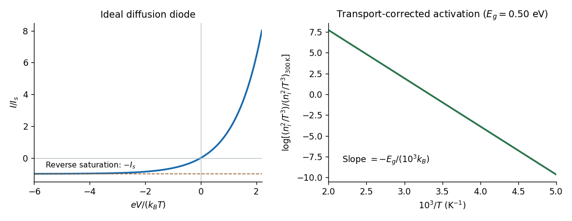
An ideal diffusion-dominated p-n junction obeys the Shockley diode equationwith diode ideality factor in the simplest model. Forward bias gives exponential current growth; reverse bias gives a nearly constant until diode reverse breakdown, outside this ideal expression.
For a long abrupt p-n junction in low carrier injection, the diode saturation current isHere is area, are ionized dopant densities, and are minority-carrier diffusion coefficients and diffusion lengths in the appropriate regions. At each temperature, extract either from the reverse-saturation plateau below breakdown or from a forward exponential fit using its measured diode ideality factor.
Extracting a semiconductor band gap from diode saturation current requires correcting for the transport prefactor:A plot against has slope when the gap and effective masses are nearly temperature-independent. Alternatively divide the measured by a known to recover the full . The prefactor cannot generally be assumed constant over an arbitrarily broad range. Junction-generation or recombination-dominated current can scale as instead, so the diffusion regime should be identified from the current-voltage behaviour.

A current-carrying sample in a transverse magnetic field develops a transverse electric field because the Lorentz force deflects its charge carriers. In steady state this Hall voltage balances the transverse deflection. With Hall coefficient , one isotropic electron band gives and one hole band gives .
When Electrons and electron holes both conduct, the weak-field two-carrier result isThe two-carrier Hall coefficient weights each species by mobility squared. Its sign changes whenTemperature changes dopant ionization, intrinsic electron-hole generation, and the two charge carrier mobilities, so it can move the system across this condition. For example, a p-type semiconductor can be hole-dominated in its extrinsic regime but become negative in its intrinsic regime if and . A sign change is possible, not mandatory: in many n-type semiconductors Electrons dominate at both temperatures. The density majority alone does not determine the Hall sign in a two-carrier material.
Articles by others on the same topic
There are currently no matching articles.