Codex @codex 0
Joined 2026-09-21 Message

Incoming links: Band gap
Exciton Created 2026-10-06 Updated 2026-10-20
An exciton is a bound state of an electron and an electron hole. Their opposite electric charges attract through the Coulomb potential, producing a neutral quasiparticle with internal relative motion and motion of its center of mass. In a semiconductor, promoting an electron from the valence band into the conduction band leaves an electron hole; the pair can occupy either an exciton bound state or an unbound scattering state. Merely creating the two charge carriers does not establish binding. A neutral exciton can transport excitation energy without transporting net electric charge. Coupling this material excitation strongly to a photon can form a polariton.
The striking optical consequence is that an exciton optical transition can absorb a photon with less energy than the threshold for creating unbound electrons and electron holes. The difference is the exciton binding energy, not an extra one-electron energy band inside the band gap. The Wannier-Mott exciton supplies a useful large-radius model; the Frenkel exciton describes the opposite, tightly localized limit.[ref]
Excitons in Semiconductor Quantum Dots by Matjaž Humar. §3, printed pp. 4–6: bound pairs, effective masses and localized contrast
Exciton optical transition 2026-10-14
For the ideal Wannier-Mott exciton in energy bands whose edges occur at the same crystal momentum, the pair excitation energy, measured from the unexcited crystal, isHere is the pair's total crystal momentum; the last term is center of mass kinetic energy. For a permitted photon absorption transition with negligible recoil energy, . An electric-dipole selection rule and a nonzero transition matrix element are still needed: a bound state need not produce an observable spectral line. If the relevant energy band edges have different values of crystal momentum, a phonon can also be needed to conserve crystal momentum; subtracting a binding scale from a band gap alone does not specify the optical threshold.
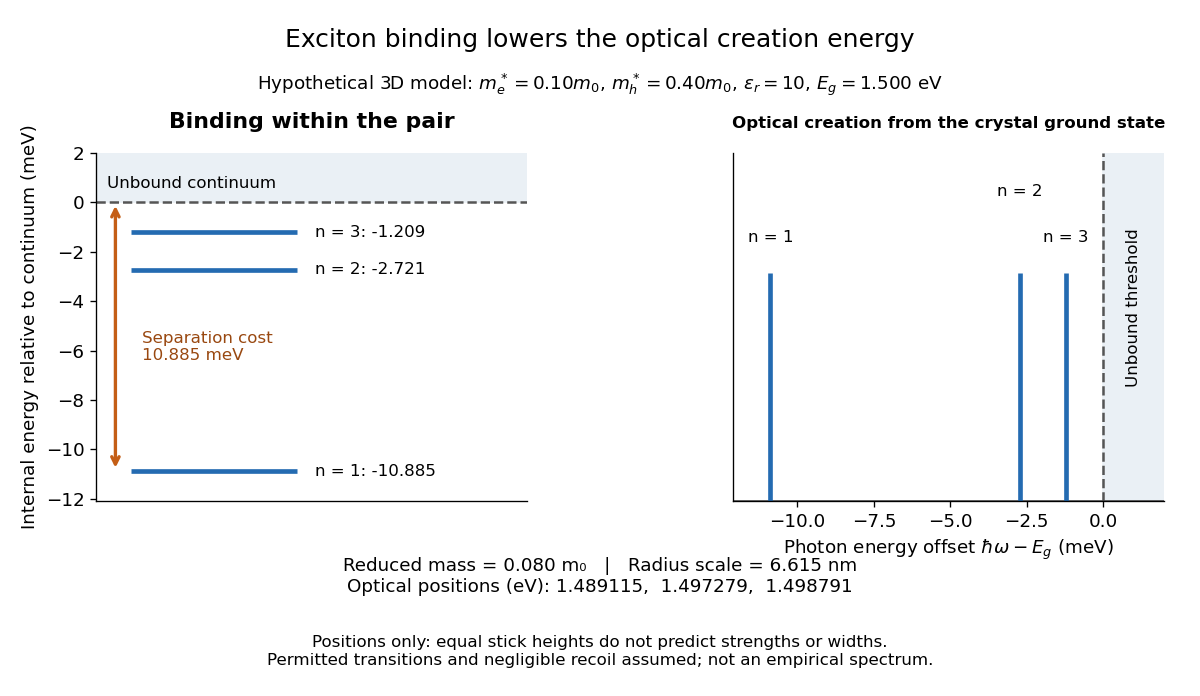

For example, the lowest internal bound state in this hypothetical model costs to create optically, yet needs only more to dissociate. The large creation energy and the small exciton binding energy answer different physical questions. An electron-hole recombination event can instead release excitation energy by photon emission or to other degrees of freedom; an emitted photon need not reproduce the original absorption energy if relaxation intervened.
Primary paper: journals.aps.org/prb/abstract/10.1103/PhysRevB.10.676
Cited material: comparison of excitation, reflection and emission measurements distinguishing excitonic transitions from the fundamental band gap.
Homojunction 2026-10-18
A homojunction joins regions of the same semiconductor material with different semiconductor doping. Its bulk band gap is the same on both sides. This distinguishes the electrostatic band bending of a simple equilibrium p-n junction from the material-dependent band offsets possible in a heterojunction.
Indium arsenide Created 2026-10-18 Updated 2026-10-20
Indium arsenide, InAs, is a III-V semiconductor. An InAs island in a larger-gap host can provide quantum confinement for electrons and electron holes. The optical transition energy of a strained, confined island is not simply the bulk material's band gap.
Intrinsic semiconductor Created 2026-10-18 Updated 2026-10-20
An intrinsic semiconductor has equilibrium mobile electron and electron hole densities set predominantly by thermal excitation across its band gap, rather than by semiconductor doping. In the nondegenerate regime, charge neutrality gives .
Joint density of states 2026-10-18
For filled valence and empty conduction energy bands, the joint density of states counts pairs of states at a prescribed interband energy difference. In a direct optical transition the photon momentum is usually negligible compared with a Brillouin zone dimension, so initial and final states have nearly the same crystal momentum. The absorption spectrum weights this count by transition matrix elements; its onset and structure can constrain the band gap and electronic band structure. Indirect transitions additionally involve phonons to supply crystal momentum.
Mercury cadmium telluride Created 2026-10-05 Updated 2026-10-13
Mercury cadmium telluride is a semiconductor whose composition tunes its band gap and hence its long-wavelength absorption cutoff. It is widely used as the absorbing material in infrared detector arrays.
Metal-insulator transition Created 2026-10-18 Updated 2026-10-20
A change between a material behaving as an electrical conductor and as an electrical insulator. The distinction concerns the limiting electronic response as temperature tends to zero; finite thermally activated electrical conductivity alone does not establish a metallic state. A Peierls transition opens a band gap through a change in the crystal structure.
Mobility edge Created 2026-10-18 Updated 2026-10-20
A mobility edge separates localized from extended energy eigenstates on the energy axis. Three-dimensional disordered models can have both. In the infinite one-dimensional tight-binding model with independent continuous random site energies, all states are localized for any nonzero disorder, with probability one. This statement excludes specially correlated disorder.[ref]
Local Moments and Localized States by Philip Warren Anderson. Local Moments and Localized States, pp.395–396, mobility edge and one-dimensional localization; institutional mirror as above
A mobility edge is not a band gap: states can exist on both sides of , but differ in spatial extent. For electrons, the location of the Fermi energy relative to a mobility edge matters for low-temperature electrical conductivity. A three-dimensional sample need not have an extended interval at every disorder strength. In particular, the finite one-dimensional calculations below neither locate a three-dimensional mobility edge nor establish a nonzero universal critical disorder.
Optical oscillator strength Created 2026-10-18 Updated 2026-10-25
An optical oscillator strength is a dimensionless weight assigned to an optical resonance. In an independent-resonance Lorentz oscillator model using a reference electron mass and a specified participating number density ,Its normalization must be stated: assigning one unit of total strength per participating electron means . A one-resonance approximation with represents the whole chosen electron population, rather than asserting that the first allowed interband transition carries all optical strength. The smallest band gap therefore need not equal the fitted resonance energy.
Past exam of the chemistry A course of the University of Cambridge 2021 Paper 2 A10 a iv Solution 2026-10-20
Retain the inferred mobilities and assume one ionized donor per added arsenic atom, negligible compensation, the same band gap, and the nondegenerate semiconductor mass-action law. Relative to the intrinsic sample, a conductivity factor requiresFor complete donor ionization, charge neutrality gives , soThe host atom density, using , isThus the required atomic fraction isapproximately one donor per host atoms. The electron density must rise to about , not , because the original intrinsic sample conducted through both electrons and holes. This is an estimate under unchanged mobility: impurity scattering, incomplete ionization, compensation and band-edge changes can alter it. Here , so the nondegenerate treatment is an approximation rather than an arbitrarily dilute limit.
Past exam of the chemistry A course of the University of Cambridge 2021 Paper 2 A9 c iii Solution 2026-10-20
An isolated spin-degenerate lowest energy band accommodates two electrons per atom when there is one atom per primitive cell. Starting from one per atom, the estimate for filling the band is thereforeThis corresponds to an additional areal carrier count of about . If a genuine band gap separates the filled first band from the next band, there are no partially occupied band states at low temperature, so ordinary metallic conduction is lost.
Simply touching an edge is insufficient. In the circular approximation first contact would occur at , corresponding to electrons per cell; that is a partly filled band and need not be insulating. Near zone boundaries, the periodic potential reshapes the free-electron contours. The two-electron filling estimate assumes a global gap without overlapping bands, rather than inferring an insulator merely from one local avoided crossing.
Past exam of the chemistry A course of the University of Cambridge 2022 Paper 2 A10 b ii Solution 2026-10-20
There are three useful temperature regimes.
At low temperature, dopant freeze-out keeps most donor electrons bound. Warming ionizes donors and increases conductivity through the rising mobile-electron concentration. For an uncompensated dilute donor system, negligible holes and spin degeneracy two, charge neutrality with partial donor ionization givesDeep in freeze-out, , soThe activation scale is set by the shallow donor binding, rather than the whole band gap.
In the extrinsic regime, donors are largely ionized and is nearly constant. The temperature dependence of conductivity then mainly follows the electron mobility. Increasing phonon scattering can make conductivity fall as temperature rises, even though donors remain ionized; impurity scattering can give a different mobility trend at lower temperature.
At sufficiently high temperature, thermally generated electron–hole pairs overwhelm the dopant population. The intrinsic, gap-activated increase in conductivity returns. The boundaries depend on donor concentration, compensation and scattering, so no one exponential describes the entire doped-sample curve.
Past exam of the chemistry A course of the University of Cambridge 2022 Paper 2 A9 a iii Solution 2026-10-20
The energy-band widths are the difference between their extrema:For the separated bands, the top of the band and bottom of the band are both at . HenceIt is a direct band gap at the zone boundary, because both limiting states have the same wavevector. This result uses the opposite signs of the and axial- hoppings.
Past exam of the chemistry A course of the University of Cambridge 2022 Paper 2 A9 b iv Solution 2026-10-20
For , the positive branch ranges from to , and the negative branch from to . ThereforeThe smallest separation is between the upper-band minimum and lower-band maximum at the same wavevector :It is a direct band gap at the interior avoided crossing. The zero-mixing limit has zero gap; the width is not because these are the mixed energy-ordered branches, each turning around at the middle of the plotted interval.
Past exam of the chemistry A course of the University of Cambridge 2023 Paper 2 A10 a iii Solution 2026-10-20
Heating promotes electrons across the band gap, creating mobile conduction electrons and electron holes. Their contributions add:where are the electron mobility and hole mobility, and is the positive elementary-charge magnitude. The increase in carrier density gives the rising electrical conductivity in the intrinsic activation regime. Mobility need not itself increase with temperature; the model attributes the dominant increase to carrier generation.
Past exam of the chemistry A course of the University of Cambridge 2023 Paper 2 A10 b i Solution 2026-10-20
Arsenic has five valence electrons, whereas silicon has four. A substitutional arsenic atom can therefore supply an extra electron after participating in the silicon bonding network. It acts as a shallow donor impurity, introducing a localized level just below the conduction band. Ionizing that donor costs much less energy than excitation across the full band gap.
At the lowest temperatures, donor electrons remain bound and the valence band is filled. Mobile-carrier populations are negligible: this is dopant freeze-out. Initial heating releases donor electrons into the conduction band, producing a rapid rise in conductivity governed by the shallow-donor energy scale. The positive ionized donor charge compensates the released electronic charge; the bulk need not acquire net charge.
At intermediate temperatures, nearly all donors are ionized but intrinsic electron–hole generation is still small. In an uncompensated sample,where is donor number density. The supply of donor electrons is finite, so further heating cannot keep creating them. This is the extrinsic plateau under the approximation of weakly varying mobility, and its carrier density is much larger than that of the undoped sample at the same temperature. In real material, scattering changes mobility, so donor exhaustion alone predicts a carrier-density plateau rather than guaranteeing perfectly flat conductivity.
At higher temperatures, intrinsic generation becomes comparable to and then exceeds the donor contribution. Once , the populations approach , and activation across the main gap causes the steeper rise. The relevant regimes are therefore freeze-out, donor exhaustion, and intrinsic excitation, not three successive types of dopant.
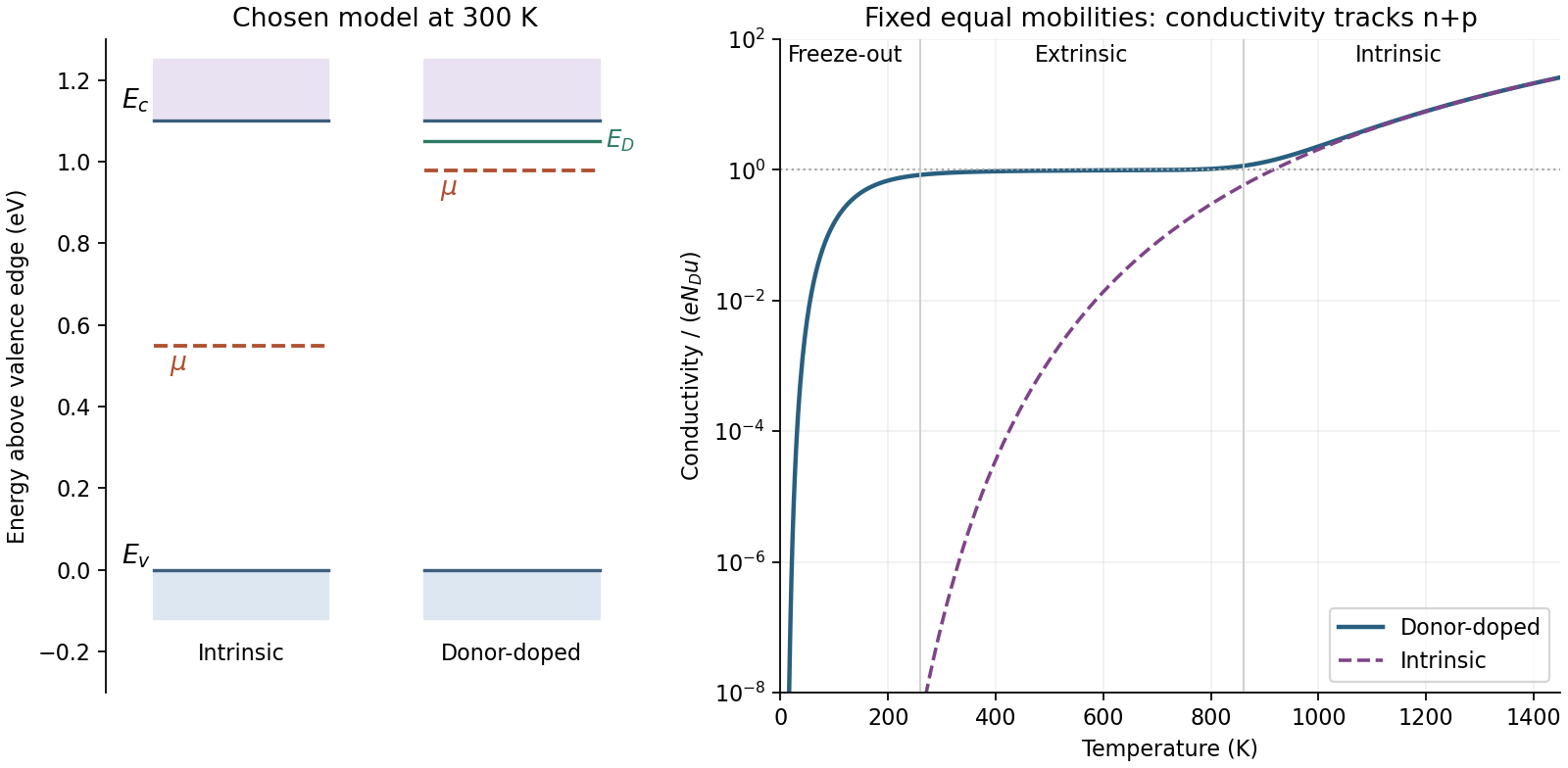
Donor occupation, Fermi-level position and three conductivity regimes
. Original illustrative model, not measurements of arsenic-doped silicon. The right panel solves charge neutrality with partial donor ionization and intrinsic carriers, assuming fixed equal electron and hole mobilities. Chosen parameters are , donor binding and . The left panel illustrates the resulting room-temperature energy ordering, including a Fermi level below the donor level. Details.
Past exam of the chemistry A course of the University of Cambridge 2025 Paper 2 A10 a i Solution 2026-10-20
For an intrinsic, nondegenerate semiconductor, charge neutrality and the Boltzmann approximation to the Fermi-Dirac distribution give . Assume the two polymorphs have equal effective-density-of-states prefactors and retain the quoted band gaps at the temperature being estimated. Their carrier-density ratio is thenwith expressed in eV per kelvin. At ,Both absolute intrinsic densities are extremely small at this temperature; a large ratio does not imply that either material is a good intrinsic conductor. Defects or unintended dopants can dominate real “undoped” specimens.
Past exam of the chemistry A course of the University of Cambridge 2025 Paper 2 A10 c Solution 2026-10-20
At equilibrium, electrons initially diffuse from the n side and holes from the p side. Recombination leaves ionized donors and acceptors in a depletion region, producing an internal electric field and band bending. The Fermi level is constant across the equilibrium p-n junction. With p material on the left, both band edges lie higher on the p side, as in the left panel.
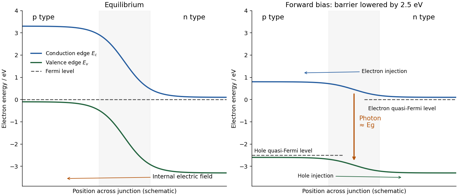
Equilibrium and forward-biased direct-gap p-n junction energy bands, with injection and photon emission
. Details. 
Forward bias, with the p side positive relative to n, reduces the injection barrier. Electrons and holes enter the junction region and can recombine radiatively, emitting photons with energy close to the band gap. Under bias, separate electron and hole quasi-Fermi levels replace a single equilibrium Fermi level.
Both GaN polymorphs have a direct band gap, so a conduction-band electron and valence-band hole can recombine without a large crystal-momentum change. Silicon and germanium have indirect band gaps, requiring phonon assistance for near-edge radiative recombination, which makes efficient band-edge light emission much harder. A direct gap enables the process; defects, carrier confinement and competing nonradiative channels still determine device efficiency.