A forward-biased p-n junction injects electrons from its n-type semiconductor and electron holes from its p-type semiconductor into an active region. A direct band gap allows radiative transitions without a compensating phonon, so stimulated emission can compete effectively with nonradiative processes. At thermal equilibrium there is one Fermi level; forward injection instead establishes separate electron and valence-electron quasi-Fermi levels and . Sufficient injection makes conduction states more occupied than the corresponding valence states, producing optical gain.
Two parallel cleaved facets supply an optical resonator. At normal incidence their approximate intensity reflectance follows the Fresnel equations:A resonant normal mode grows when its round-trip amplification exceeds its losses. For length , material optical gain , overlap factor , internal intensity loss and facet reflectances ,The pump supplies the emitted energy; the facets provide feedback and let some output escape. Positive optical gain alone does not establish laser threshold.
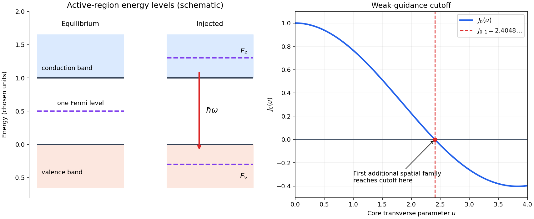
Injected laser diode levels and the first additional guided spatial mode
. Original schematic: the left panel uses stipulated energy units to distinguish equilibrium and injected quasi-Fermi levels, with an allowed downward optical transition. The right panel plots , whose first zero fixes the weak-guidance spatial-mode cutoff. The separate panels do not represent a shared spatial coordinate. Details.
For a vertical interband transition, the crystal momentum is effectively unchanged because the photon momentum is small. A stimulated downward transition needs an occupied upper state and an empty lower state, with factor ; upward photon absorption has factor . The two matrix elements agree by microscopic reversibility. Their difference is thereforeA common slowly varying transition-strength factor is implicit. Broadening replaces the sharp transition by a convolution; multiple valence bands contribute separate terms.
For one isotropic pair of parabolic energy bands, writeThus . Including the usual twofold spin degeneracy, the number of paired states per volume inside a sphere of radius is . Differentiating with respect to transition energy gives the three-dimensional parabolic interband joint density of statesFor density per angular frequency, . Stating the density convention avoids a missing factor of ; other degeneracies multiply the formula.
At a common carrier temperature, the Fermi-Dirac distribution is a strictly decreasing function of . The direct-gap semiconductor gain condition follows:The lower inequality denotes a transition above the ideal band edge, where the displayed joint density of states is nonzero. Thus quasi-Fermi-level splitting must exceed the transition photon energy. Equality is transparency, rather than net amplification; at zero temperature an allowed transition must also lie within the occupied-electron and empty-valence windows.
Adjacent longitudinal cavity modes obey . Neglecting optical dispersion in estimating their spacing,Hence the gain interval accommodatespossible longitudinal cavity modes. The exact integer depends on the positions of the interval endpoints and resonances. This counts available resonances; mode competition and actual laser threshold can reduce the number that oscillates. More accurately, the spacing uses the group refractive index instead of .
A broad multimode spectrum suffers differential delay through optical fiber group velocity dispersion, broadening transmitted pulses. Near , ordinary silica optical fiber attenuation is also larger than in the long-distance windows near and . These limitations concern this short-wavelength, simple multimode device: suitably engineered single-frequency semiconductor lasers at telecommunications wavelengths are useful communication sources.
A double heterostructure laser places a lower-band gap active layer between wider-band gap layers with suitable type-I band alignment. The band offsets confine injected electrons and electron holes in the same small volume, increasing their overlap and reducing escape. Usually the active layer also has larger refractive index, so the same sandwich forms an optical waveguide. Optical confinement increases the gain-overlap factor , while carrier confinement lowers the injection needed to reach the required quasi-Fermi-level splitting. These two distinct mechanisms reduce threshold current and heating. A band gap difference alone does not establish the sign of both confinement barriers; suitable band offsets are essential.
Articles by others on the same topic
There are currently no matching articles.