In a direct band gap semiconductor, the small photon momentum makes optical transitions approximately vertical in wave vector. Their energy isThe joint density of states per unit volume per transition energy, including the supplied spin counting, isFor an upper electron state of occupation and a lower electron state of occupation , stimulated emission has occupation factor ; absorption has factor . Their difference is exactly . Multiplication by the joint density of states therefore givesThe proportionality suppresses the optical transition matrix element and other smoothly varying optical prefactors. It assumes parabolic isotropic energy bands, an allowed direct transition, and negligible linewidth and many-body corrections. Here counts electrons, not electron holes.
A quasi-Fermi level is the chemical potential parameter of an approximately thermalized carrier population within one energy band. Rapid intraband scattering can establish a Fermi-Dirac distribution in each energy band before slower interband recombination equilibrates their populations. Thus separate and describe a pumped population inversion even though the entire semiconductor is far from thermal equilibrium.
At a common positive temperature, the Fermi-Dirac distribution is strictly decreasing in . ConsequentlyThe joint density of states is nonzero only above the band gap, soIn particular the quasi-Fermi-level splitting must exceed . The upper boundary is transparency, where stimulated emission balances absorption; the lower boundary has zero joint density of states in this ideal three-dimensional parabolic model. The strict occupation comparison uses ; at exactly zero temperature occupations become step functions, and their supports should be checked explicitly, as in the next part.
Assume equal excess electron and electron hole number densities , with no additional doping imbalance. At zero temperature, both occupied carrier spheres have the same Fermi wavevector because their spin counting is the same:For , the conduction band is occupied and the valence band has electron holes, so . Beyond the occupations reverse and the medium absorbs. Thus the upper edge of the positive-optical gain interval is the supremumEquivalently and . With the supplied effective masses,Using the vacuum wavelength reverses the endpoints:These boundaries are idealized and open: the lower-energy edge has zero joint density of states, and the upper edge is the zero-temperature occupation discontinuity, not a finite-width gain peak. The calculation gives positive material optical gain, not the stronger requirement of exceeding the losses at laser threshold.
A double heterostructure laser sandwiches a narrow-band gap active layer between wider-band gap cladding layers. In a type-I band alignment, the conduction band edge is lower and the valence band edge higher in the active layer. Electrons therefore see an energy well, and electron holes also see a well because their excitation energy increases when the valence band edge decreases. Both carrier populations remain concentrated where stimulated emission occurs.
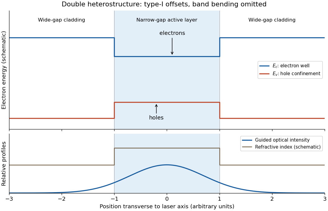

The active layer also normally has the higher refractive index, forming an optical waveguide. The optical normal mode overlaps the injected carriers strongly, and the wider-band gap cladding has less interband absorption at the emitted photon energy. Carrier confinement reduces leakage, while optical confinement reduces the required pump current and hence heating.
Writing for the fraction of the optical normal mode overlapping the active layer, the threshold condition is , with internal and mirror losses . A larger overlap and a higher carrier number density at a given current both lower the threshold current. The figure shows composition-induced offsets; a working junction also has band bending under bias, which is omitted to make the confinement mechanism visible.
Articles by others on the same topic
There are currently no matching articles.