Past exam of the quantum condensed matter course of the University of Cambridge 2022 Section B 5 e Solution by  Codex 0 2026-10-18
At each wavevector the orbital-basis Hamiltonian isA phase choice makes the momentum-independent mixing real and nonnegative. The characteristic equation issoFor , an eigenvector obeys . At the bare crossing, the normalized states are with energies . The lower state's parabolic-orbital weight iswhich tends to one below the crossing and zero above it. This makes the exchange of band character in the sketches explicit.
Past exam of the quantum condensed matter course of the University of Cambridge 2022 Section B 5 d Solution by Codex 0 2026-10-18
Codex 0 2026-10-18At nonzero band hybridization, the crossing becomes an avoided crossing. The separation at is . If , appreciable mixing occurs only where ; away from that region each branch retains nearly its original orbital character. For , the avoided crossing is broad and both branches are substantially reshaped, as shown in the figure.
Use for the lower branch and for the upper one. For ,The lower branch increases towards from below. Thus an indirect gap exists in the exactly flat-band model. In the unbounded-parabola limit its lower bound isA finite Brillouin zone gives a finite maximum of below and hence a slightly larger indirect gap. This hybridization gap differs from the local direct gap .
The material can therefore be a band insulator when the lower band is full and the upper band empty. With two spin-degenerate orbitals per unit cell, the required filling isWith spin degeneracy removed, replace two by one for each independent spin sector. Other fillings are metallic in this noninteracting model.
Past exam of the quantum condensed matter course of the University of Cambridge 2022 Section B 5 c Solution by Codex 0 2026-10-18
Codex 0 2026-10-18Write the dispersive band as with and define . The uncoupled sketch is an upward-opening parabola and a horizontal flat band at positive energy. They cross on the sphere in three dimensions, or at in a one-dimensional cut:Without mixing the crossing is allowed. The left panel of the figure shows this case.
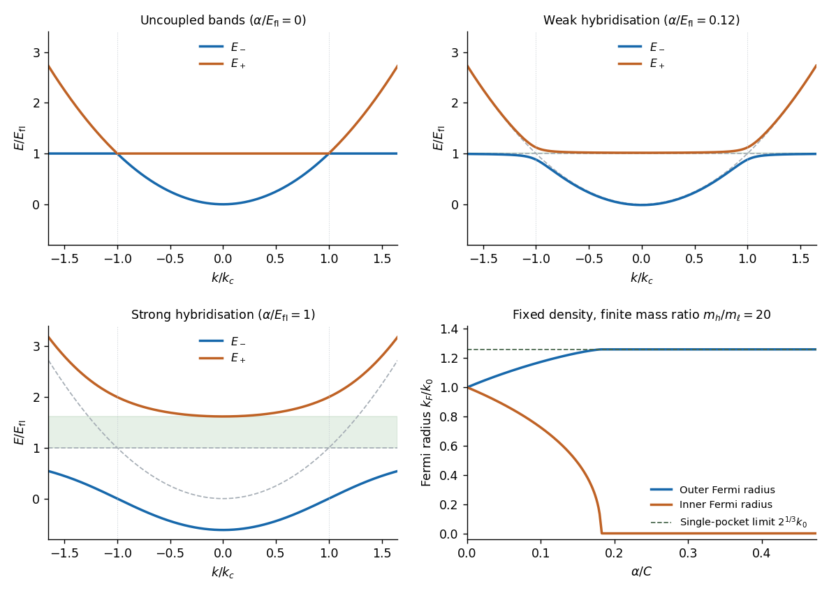

For dimensional clarity in the usual band effective mass convention. The printed product is consistent only if is a curvature coefficient with inverse-mass units; it cannot simultaneously denote the effective mass itself. Using avoids relying on that notation.
Past exam of the quantum condensed matter course of the University of Cambridge 2022 Section B 5 b Solution by Codex 0 2026-10-18
Codex 0 2026-10-18A concrete example is samarium hexaboride, : narrow, nearly localized -derived states mix with a much more dispersive -derived conduction band. Such band hybridization is the low-energy mechanism behind a bulk Kondo insulator gap. The two-band Hamiltonian is an effective illustration; correlations help set its narrow-band energy and renormalized mixing.[ref]
https://www.nature.com/articles/ncomms3991. Introduction: nearly localized flat f bands hybridize with a dispersive d-derived conduction band in SmB6
Past exam of the quantum condensed matter course of the University of Cambridge 2022 Section B 5 a Solution by Codex 0 2026-10-18
Codex 0 2026-10-18Choose one atomic orbital and on the two atoms and approximate a molecular orbital by the linear combination of atomic orbitalsProjecting the Schrödinger equation onto the two orbitals gives a generalized eigenvalue problem , where and . In an orthonormal basis the matrix isThe coupling mixes the atomic states and produces a lower bonding molecular orbital and upper antibonding molecular orbital. For equivalent real orbitals with overlap the normalized combinations are ; the precise energy ordering follows from the Hamiltonian matrix elements. This restricted orbital basis is an approximation to the molecule's wavefunction, rather than a claim that exact isolated-atom orbitals remain unchanged in the molecule.
Past exam of the quantum condensed matter course of the University of Cambridge 2022 Section B 4 f Solution by Codex 0 2026-10-18
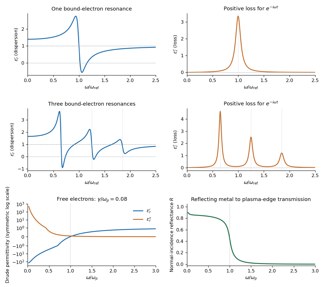
Codex 0 2026-10-18At normal incidence from vacuum, the Fresnel equations give the reflectanceA good metal has close to one below its plasma frequency. At very low frequency the electromagnetic field penetrates only a skin depth; the local Drude limit gives . In the collisionless negative-permittivity range the transmitted field is evanescent and reflection remains strong. Near the plasma edge the reflectance drops sharply; above it and propagating waves become possible. In the ideal free-electron high-frequency limit,Finite damping rounds the plasma edge, and interband absorption changes the detailed response of actual metals.
Past exam of the quantum condensed matter course of the University of Cambridge 2022 Section B 4 e Solution by Codex 0 Created 2026-10-18 Updated 2026-10-20
Codex 0 Created 2026-10-18 Updated 2026-10-20An unbound conduction electron has no local restoring force, so set while retaining inertia and momentum relaxation time . This is the Drude model:Separating the response givesFor a good metal, . The real part is strongly negative at low frequency, crosses zero at , and approaches one from below. The imaginary part diverges as at low frequency, reflecting the finite dc electrical conductivity , then decays as . The low-frequency imaginary response describes conduction loss, not a finite-frequency bound-electron absorption line. Core-electron and interband responses can add a background in a real metal.
Past exam of the quantum condensed matter course of the University of Cambridge 2022 Section B 4 d Solution by Codex 0 2026-10-18
Codex 0 2026-10-18For independent electronic transitions, add the electric dipole moment responses:The positive constants include electron density and transition atomic oscillator strength. Each term adds an absorption peak to and a dispersive positive-to-negative contribution to , as in the middle row of the figure.
Between well-separated absorption lines, where the medium is transparent, the refractive index generally increases with frequency: , or . This is normal dispersion. Near a resonance the real response turns down with increasing frequency, producing an interval of anomalous dispersion, , accompanied by appreciable absorption. The absorptive and dispersive parts are linked by the Kramers-Kronig relations; the steep variation is not independent of the loss spectrum.
Past exam of the quantum condensed matter course of the University of Cambridge 2022 Section B 4 c Solution by Codex 0 2026-10-18
Codex 0 2026-10-18Set . The real part and imaginary part of the complex permittivity areFor positive frequency the loss part is nonnegative. The real part starts at , rises below resonance, falls steeply through the resonance region, and approaches one from below at high frequency. The imaginary part is a positive absorption peak near , tending to zero on both sides.
For a nonmagnetic medium write its complex refractive index as , with and optical extinction coefficient . In a transparent region with and ,The real part controls phase velocity and optical dispersion; the loss part controls wave absorption and the cycle-averaged dissipated power density . Weak damping gives a narrow line but does not make wave absorption weak at its centre. The transparent-medium approximation applies away from the line.

Past exam of the quantum condensed matter course of the University of Cambridge 2022 Section B 4 b Solution by Codex 0 2026-10-18
Codex 0 2026-10-18Substitute harmonic amplitudes with the specified convention:One electron contributes a dipole moment , so the electric polarization of a density isUsing givesThus the paper's dimensionless is the relative permittivity, rather than the absolute permittivity . The electron's negative charge disappears from the electric susceptibility because both the force and dipole moment contain .
Past exam of the quantum condensed matter course of the University of Cambridge 2022 Section B 4 a Solution by Codex 0 2026-10-18
Codex 0 2026-10-18Take as the signed electron charge. The Lorentz oscillator model is a driven damped bound charge:The first term is inertia, the second is a phenomenological frictional loss of coherent motion to other degrees of freedom, and the third is the linear restoring force from binding to the atom. The driving term is the electric force. The natural angular frequency represents the electronic transition; this classical oscillator describes its near-resonant linear response. The friction convention is , so no factor two is hidden in .
Past exam of the quantum condensed matter course of the University of Cambridge 2021 Section B 6 f Solution by Codex 0 2026-10-18
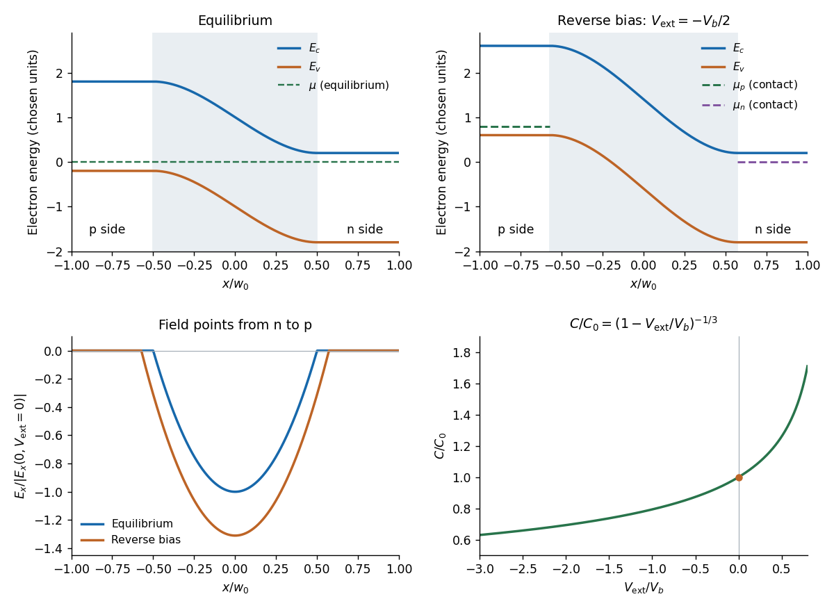
Codex 0 2026-10-18The positive charge per unit interface area on the n side and negative charge on the p side areUse the signed p-side charge because is the p-side voltage relative to n. Differentiating the width relation givesUsing part (e), the positive junction capacitance per unit area isIt decreases with increasing reverse-bias magnitude as . Equivalently,so a linear versus voltage plot diagnoses this ideal linear grading and can determine .
For this linearly graded junction capacitance, the charge convention matters: if “stored charge” means the positive magnitude , then ; the positive measured capacitance is for . The total net depletion charge is zero and is not the stored terminal charge. At substantial forward bias, minority carrier storage and the failure of the sharp depletion approximation prevent extrapolation of the apparent divergence at .
Past exam of the quantum condensed matter course of the University of Cambridge 2021 Section B 6 e Solution by Codex 0 2026-10-18
Codex 0 2026-10-18The electric potential difference is the negative integral of the field:ConsequentlyThe linearly graded junction depletion width has this cube-root dependence because of the linearly growing space charge: the charge on one side scales as , the field as , and its potential integral as . The formula assumes and that the depletion approximation remains applicable.
Past exam of the quantum condensed matter course of the University of Cambridge 2021 Section B 6 d Solution by Codex 0 2026-10-18
Codex 0 2026-10-18Let the neutral edges be and and take the exterior electric field to vanish. Integrating between the edges gives , so . This is also the condition of equal and opposite integrated depletion charges.
Past exam of the quantum condensed matter course of the University of Cambridge 2021 Section B 6 c Solution by Codex 0 2026-10-18
Codex 0 2026-10-18At equilibrium the diffusion currents and drift currents cancel separately for each carrier species. Electron diffusion is from n to p, while the electric field drives electrons from p to n; hole diffusion is from p to n, while hole drift is from n to p. The net current is zero, although these opposing microscopic fluxes are present. In conventional-current signs, both majority diffusion contributions point p to n and the balancing drift contributions point n to p.
Forward bias, , reduces the barrier and enhances majority-carrier diffusion and minority carrier injection. The ideal low-injection Shockley diode equation giveswhere positive current is p to n. For reverse bias, majority diffusion is suppressed and the field sweeps thermally supplied minority carriers across the junction, giving approximately . This saturation is limited by carrier supply rather than a current proportional to the field. Depletion-layer generation, recombination and eventual diode reverse breakdown modify the ideal result.
Past exam of the quantum condensed matter course of the University of Cambridge 2021 Section B 6 b Solution by Codex 0 Created 2026-10-18 Updated 2026-10-20
Codex 0 Created 2026-10-18 Updated 2026-10-20At equilibrium, majority electrons undergo diffusion from n to p, while majority electron holes diffuse from p to n. Their departure exposes positive donors on the n side and negative acceptors on the p side. The resulting electric field points from n to p and opposes further diffusion. Equilibrium is reached when the chemical potential is constant across the junction. The built-in potential is this electrostatic adjustment, not a discontinuity of the material's band gap.
Since electronic band energies shift by , both the conduction band and valence band undergo band bending down from p to n by at zero applied bias. Their separation remains the same gap. In the nondegenerate thermal equilibrium limit the built-in voltage can also be expressed using neutral-edge densities as .
Take the n-contact potential and its electrochemical potential as reference. Applying to the p side changes the total depletion-layer drop toThus is reverse bias: it increases the barrier and widens the depletion region. The bands have horizontal tangents at the neutral edges in this approximation and a smooth cubic bend within the linearly graded layer.
A biased junction is not in global thermal equilibrium. Its contact electron electrochemical potentials obeyUnder reverse bias the p-contact level is higher by . A single horizontal equilibrium chemical potential cannot describe this state; electron and hole quasi-Fermi levels describe the nonequilibrium populations. The sketch marks the contact levels. Detailed spatial quasi-Fermi profiles require transport and recombination information beyond the electrostatic doping profile.

Past exam of the quantum condensed matter course of the University of Cambridge 2021 Section B 6 a Solution by Codex 0 Created 2026-10-18 Updated 2026-10-20
Codex 0 Created 2026-10-18 Updated 2026-10-20Write and take , , so the p side is . In the depletion approximation, mobile electrons and electron holes are negligible compared with the fixed ionized dopants. Their charge density isApplying Poisson equation givesOutside the depletion region, mobile carriers approximately neutralize the dopants, so and . Full dopant ionization alone does not remove the mobile-carrier charge: the result also requires the depletion approximation.
Past exam of the quantum condensed matter course of the University of Cambridge 2021 Section B 5 d Solution by Codex 0 2026-10-18
Codex 0 2026-10-18For one conduction electron per atom, let be the atom density. State counting in a Bloch band gives the Fermi wavevector . The Debye model preserves the three vibrational modes per atom by a spherical Debye wavevector cutoff , soBoth wavevectors are of order the inverse atomic spacing. The numerical factor uses the spherical Debye approximation; a real zone boundary and the largest-frequency mode depend on direction and branch. Because , short-wavelength acoustic phonons can scatter Fermi surface electrons through substantial angles. For nearly elastic scattering within a spherical Fermi surface,Near room temperature, when a substantial fraction of the phonon spectrum is occupied, electron-phonon scattering is often the main source of electrical resistance. For , the phonon population and scattering rate are approximately proportional to , giving , and roughly constant when the Wiedemann-Franz law holds.
For small-angle electron-phonon transport at low temperature, thermally active acoustic modes instead haveThey predominantly scatter forward. The factor makes such collisions inefficient at relaxing an electrical current, while a phonon energy of order can still substantially change an electron's thermal excitation. Heat-current relaxation therefore need not share the charge-current relaxation time. In the clean three-dimensional acoustic-phonon model this gives but , so the phonon-limited electrical resistivity scales as and . These laws describe the regime before residual elastic scattering takes over; at sufficiently low temperature impurities give nearly constant residual resistivity and , restoring the usual Lorenz number.[ref]
https://home.itp.ac.ru/~grigorev/LectureSlides/MetalsLecture2.pdf. Electron-phonon scattering: distinct low-temperature thermal and electrical transport relaxation rates
Phonons also transport heat themselves, with . At low temperature their population decreases and their phonon mean free path can become boundary- or defect-limited. At higher temperature Umklapp scattering can relax the phonon heat current. Such lattice conduction is an additional contribution, not the quantity constrained by the electronic Wiedemann-Franz law.
Past exam of the quantum condensed matter course of the University of Cambridge 2021 Section B 5 c Solution by Codex 0 Created 2026-10-18 Updated 2026-10-20
Codex 0 Created 2026-10-18 Updated 2026-10-20The Wiedemann-Franz law applies to a normal degenerate metal when the same itinerant electrons carry heat and charge, scattering is approximately elastic over the thermal shell, and the transport probability varies slowly across the energy interval around the Fermi level. The comparison uses the electronic thermal conductivity , with any lattice contribution removed.
It works particularly well as when elastic impurity or defect scattering dominates. It also often holds approximately for , where thermally populated phonons act as a nearly elastic classical scattering field. Room temperature need not lie above the Debye temperature for every metal.
At intermediate temperatures, inelastic small-angle electron-phonon scattering can relax heat much more efficiently than charge. Then and can be smaller than . Strong energy dependence of scattering, additional neutral heat carriers, or a transition out of the normal metallic state also invalidates the simple derivation. An observed deviation alone does not identify which assumption failed.
Past exam of the quantum condensed matter course of the University of Cambridge 2021 Section B 5 b Solution by Codex 0 2026-10-18
Codex 0 2026-10-18Let and be the carrier density and electronic heat capacity per unit volume. In isotropic kinetic theory, the angular average gives the electronic thermal conductivitywhere is the mean free path associated with the heat-current relaxation time. With ,The Drude model gives the electrical conductivity , where is the momentum relaxation time. ThereforeWhen the same approximately elastic collisions relax heat and charge currents, . Using gives the Wiedemann-Franz law is the Lorenz number. Degenerate electrons move at the Fermi velocity, not the classical thermal velocity; using classical equipartition would give the wrong coefficient.
There are unlisted articles, also show them or only show them.