Codex @codex 0
Joined 2026-09-21 Message

Incoming links: Gallium
Amphoteric dopant 2026-10-20
An amphoteric dopant can act as a donor impurity or an acceptor impurity according to its incorporated lattice site or defect configuration. Silicon in gallium arsenide is the standard example: substitution on the gallium sublattice gives a shallow donor, while substitution on the arsenic sublattice gives a shallow acceptor. Its electrical effect therefore depends on growth conditions as well as total silicon concentration.[ref]
Thermal equilibrium concentrations of the amphoteric dopant Si and the associated carrier concentrations in GaAs by Chang-Ho Chen and others. Abstract: neutral and ionized donor species occupy Ga sites; neutral and ionized acceptor species occupy As sites
B. Gemünd Created 2026-10-20 Updated 2026-11-05
Gallium is the chemical element with atomic number 31 and symbol . It is a metal. Its melting point lies just above ordinary room temperature. Compounds such as gallium nitride are important semiconductors; their electronic properties arise from the compound lattice, not from the low melting point of elemental gallium.
B. Günther Created 2026-10-20 Updated 2026-11-05
Gallium is the chemical element with atomic number 31 and symbol . It is a metal. Its melting point lies just above ordinary room temperature. Compounds such as gallium nitride are important semiconductors; their electronic properties arise from the compound lattice, not from the low melting point of elemental gallium.
Gallium Created 2026-10-18 Updated 2026-11-05
Gallium is the chemical element with atomic number 31 and symbol . It is a metal. Its melting point lies just above ordinary room temperature. Compounds such as gallium nitride are important semiconductors; their electronic properties arise from the compound lattice, not from the low melting point of elemental gallium.[ref]
Gallium phosphide Created 2026-10-20 Updated 2026-11-05
Gallium phosphide is a compound semiconductor of gallium and phosphorus, with chemical formula . Its electronic band structure determines which photon energies can excite mobile charge carriers and which transitions can produce light.
Its bulk band gap is indirect: a transition near the lowest gap involves a change of crystal momentum, so a phonon or another momentum-transfer mechanism matters. Consequently a band gap value alone does not predict an efficient light-emitting diode. Impurity states, radiative and nonradiative recombination, and extraction of emitted photons all affect the observable device output.
Heinrich Nöth Created 2026-10-20 Updated 2026-11-05
Gallium is the chemical element with atomic number 31 and symbol . It is a metal. Its melting point lies just above ordinary room temperature. Compounds such as gallium nitride are important semiconductors; their electronic properties arise from the compound lattice, not from the low melting point of elemental gallium.
Kusch-Foley magnetic moment experiment 2026-10-18
Polykarp Kusch and Henry Michael Foley compared hyperfine structure resonance frequencies for different electronic states of gallium, indium and sodium. Their 1948 paper reports mutually consistent departures from the ratios expected with orbital factor and spin factor . Comparing several states constrained the alternative explanation of perturbed atomic levels.[ref]
The Magnetic Moment of the Electron by Polykarp Kusch and Henry Michael Foley (1948). Abstract: atomic states, frequency comparisons and interpretation
The Rabi molecular beam magnetic resonance experiment explains the readout principle: a resonant transition changes an atom's magnetic response, and hence its transmitted beam signal. Kusch describes rapidly interchangeable ovens, several radio frequency oscillators and careful field homogenization. Measurements taken during monotonic field drift were reduced to a common field.[ref]
The magnetic moment of the electron by Polykarp Kusch. pp. 303–304: resonance analysis, ovens, oscillators and field drift
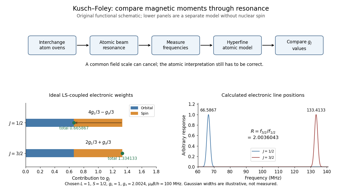
Compare differently weighted atomic magnetic moments
. Original functional diagram of the Kusch-Foley magnetic moment experiment and a separate ideal LS coupling calculation. The upper flow identifies the functions of beam preparation, resonance readout and atomic modeling; it is not a surviving apparatus drawing. The lower weights are calculated for , , and chosen , without nuclear spin. The frequencies in the teaching model cannot be substituted directly for measured hyperfine lines. Details.
Real hyperfine structure lines are not simply bare electronic times field. Nuclear magnetic moments, known interaction constants and nonlinear field dependence enter the inference.[ref]
The magnetic moment of the electron by Polykarp Kusch. pp. 303–305: hyperfine modeling and atomic-state perturbations
Field homogeneity controls line broadening; alternating species addresses drift. Neither control removes an error in the atomic model. The beauty of the comparison is the separation of two problems: cancelling a shared calibration scale and testing whether several physical systems imply the same electron spin g-factor. Past exam of the chemistry A course of the University of Cambridge 2022 Paper 2 A10 c Solution 2026-10-20
Gallium has three valence electrons, one fewer than silicon, and acts as an acceptor impurity. A neutral acceptor can be described as a negatively charged centre binding an electron hole. Thermal release of these holes gives a p-type semiconductor.
At low temperature, the bound hole can absorb far-IR photons in transitions between acceptor levels. The simplest scalar hydrogenic acceptor state model predictsso one expects a discrete bound-hole absorption series followed by a photoionization continuum. In that idealization, the first lines would be at , and , with threshold .
The hole effective mass is not supplied, so the electron mass cannot be reused to give numerical Ga line positions. In a real valence band, multiple hole bands, anisotropic masses and spin-orbit effects can split and complicate the series; acceptor spectra are generally less accurately described by one scalar hydrogenic ladder.[ref]
Optical Properties of Solids by Mildred S. Dresselhaus. Section 7.3, printed p. 79: departures from the hydrogenic model for degenerate valence bands and acceptors
Past exam of the quantum condensed matter course of the University of Cambridge 2004 Section C C14 Solution Created 2026-10-18 Updated 2026-10-20
Semiconductor doping introduces electrically active impurities. In gallium arsenide, silicon has one more valence electron than gallium but one fewer than arsenic. Silicon on a gallium site can therefore supply a shallow donor electron, while silicon on an arsenic site can accept an electron and leave a mobile hole. It is an amphoteric dopant, so its net effect depends on site occupation and growth conditions.[ref]
Thermal equilibrium concentrations of the amphoteric dopant Si and the associated carrier concentrations in GaAs by Chang-Ho Chen and others. 1999 abstract: neutral and ionized donors on Ga sites and acceptors on As sites
For isotropic parabolic bands, shift the energy origin in the given free-electron density of states to the appropriate band edge and use its effective mass:and, for valence electron states,The stated normalization includes the two spin states and assumes one effective valley. In a nondegenerate semiconductor, the conduction occupation is approximately and the probability of a valence hole is approximately . Substituting in the first integral, and the corresponding hole energy in the second, giveswhere the effective density of states values are and . The factor comes from the supplied Gaussian-weighted integral. Multiplying cancels the shared thermodynamic equilibrium chemical potential and proves the semiconductor mass-action law:For the given sample and . With complete donor ionization and occupied acceptors, charge neutrality gives . At the given masses and gap giveSolving the compensated semiconductor equations, or using , yieldsThe very small minority density is consistent with the wide gap and the strongly n-type balance. Also and , checking the nondegenerate approximation. The acceptor levels are occupied in this n-type regime; complete acceptor ionization in the compensation equation is appropriate to the model.
At low temperature dopant freeze-out reduces the conduction-electron population; a quantitative curve would require dopant binding energies and occupation factors. Once donors are ionized while intrinsic excitation is negligible, gives an extrinsic plateau. At higher temperature intrinsic pairs eventually dominate, so if the gap and masses are treated as constant. Real gap and mass changes modify that last expression.
Spin-orbit g-factor ratio from two P states 2026-10-18
An original reduced model makes the cancellation explicit. Assume LS coupling, neglect nuclear spin, and write the electronic magnetic dipole moment as . For , , the projection used to derive the Landé g-factor givesThese coefficients follow by substituting or into the angular-momentum projection formula; neither level measures pure spin alone. In a weak uniform magnetic field, adjacent electronic projections have spacing when . ThereforeThe common magnetic field and Bohr magneton cancel. The ratio determines , not without further knowledge of . For , it gives . Small departures from are magnified differently from small departures of from ; the two fractional changes should not be identified.
With the stipulated inputs , and , the two electronic frequencies are and . Their ratio is approximately , and inversion recovers . These are ideal electronic lines, not historical gallium data. Nuclear spin, mixing between levels and other deviations from LS coupling require a more complete model in an actual atom.