A quantum well confines a particle in one spatial direction while allowing motion along the layer. In a semiconductor heterostructure, band offsets can create that confinement. The following finite square well model makes the resulting discrete transverse energy levels explicit.
For one nondegenerate thermalized particle, excited-state occupation relative to the ground state is set by the excitation gap, not by the absolute energy origin. In an infinite square well of width , the first gap is . Predominant ground-state occupation requires this gap to be much larger than ; an explicit tolerated occupation gives a quantitative temperature criterion. State quantum degeneracy adds its statistical weight.
An electric field normal to a semiconductor quantum well shifts the electron and hole confinement energies and displaces their envelopes in opposite directions. The exciton optical transition usually redshifts and its oscillator strength falls as their overlap decreases. In a symmetric unbiased well the permanent dipole vanishes, so the leading weak-field shift is quadratic. This optical shift includes confinement and binding changes; it is not solely a change in exciton binding energy.
For parabolic bands confined by an infinite well of width , a same-index transition has edge . Above it the in-plane pair kinetic energy is with reduced mass .
In an infinite square well, electron and hole envelopes are the same normalized sine functions even when their effective masses differ. In the electric dipole and envelope approximations, their overlap is . The same-index rule is an ideal-envelope rule, separate from Bloch-state polarization selection rules.
A semiconductor state is approximated by a slowly varying envelope multiplying a cell-periodic Bloch function from a selected band. effective masses govern the envelope equation. Interband optical matrix elements then factor approximately into a cell-scale momentum matrix element and an envelope overlap; abrupt interfaces, band mixing and nonparabolicity limit the separation.
Consider an original one-dimensional effective mass model with for and outside. Take the same positive effective mass everywhere, an abrupt interface, and no interactions. The wavefunction represents a transverse envelope; free motion parallel to the layer is outside this calculation. A double heterostructure laser need not be thin enough for this quantization to dominate its operation.
Set , , , and . The time-independent Schrödinger equation becomesHere denotes the dimensionless potential; a bound state has . Matching the wavefunction and its derivative at givesFor the even bound state, the interior solution is and the exterior solution is . For the odd bound state, replace by and by . The physical wavefunction is .
Wavefunction normalization includes both exterior tails, not just the active layer. Direct integration givesThe first two terms are the interior integral; the last is the total exterior integral. Thus the interior probability is , with the upper sign for even parity.
Choose . There is one even root in and one odd root in ; higher branches start beyond . Each left-hand side increases on its stated interval while decreases, proving uniqueness there. Numerically,These are calculated values of the chosen finite square well. The excited bound state lies closer to the barrier and has a longer exterior tail: being bound does not mean having unit probability inside the well.
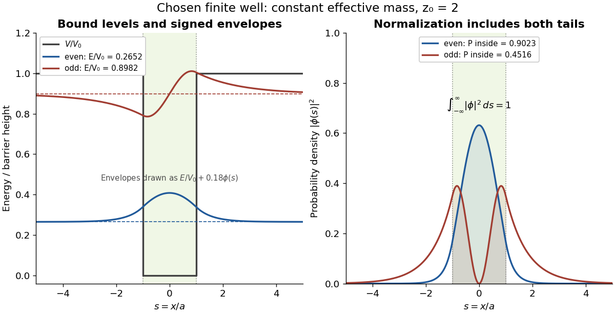
This model demonstrates electronic confinement, not optical refractive index confinement or a complete laser. Unequal effective masses, band bending, interface disorder and interactions require a more detailed model. In particular, continuity of the ordinary derivative above uses the chosen constant effective mass assumption.
Articles by others on the same topic





A quantum well is a potential energy structure where charge carriers (such as electrons and holes) are confined in a very thin region, typically on the nanometer scale. This confinement occurs in one dimension, allowing the carriers to move freely in the other two dimensions. Quantum wells are a key component in various semiconductor devices and have a significant impact on their electronic and optical properties.