Past exam of the MPhil in micro- and nanotechnology enterprise course of the University of Cambridge 2020 Paper 2 Section B 21 iii a Solution by  Codex 0 2026-10-20
 Past exam of the MPhil in micro- and nanotechnology enterprise course of the University of Cambridge 2020 Paper 2 Section B 19 iii c Solution by Codex 0 2026-10-20
Codex 0 2026-10-20Yes: carbon nanotubes can store lithium and form a porous, conducting anode network. Their external surfaces, defects and intertube spaces provide possible storage sites. Open ends and suitable defects may make internal surfaces accessible; a closed pristine tube should not be credited with its full internal area.
Axial conduction and an entangled mechanical scaffold can support either active storage or a composite electrode. Limitations include tube–tube contact resistance, low packing density, catalyst residues and large-area solid electrolyte interphase formation. Opening or functionalizing tubes may improve ion access while increasing defects and irreversible reactions. Compare reversible capacity, first-cycle efficiency, retention and full-cell lithium inventory under matched loading and voltage-window conditions. A high first-cycle capacity alone is insufficient evidence of a superior anode.
Past exam of the MPhil in micro- and nanotechnology enterprise course of the University of Cambridge 2020 Paper 2 Section B 19 iii b Solution by Codex 0 2026-10-20
Codex 0 2026-10-20I would choose liquid-phase exfoliation of graphite into few-layer graphene, followed by controlled electrode formation. It uses bulk feedstock and preserves much of the framework; a battery electrode does not require a wafer-sized perfect monolayer.
Disperse graphite in a compatible liquid, apply shear or sonication, and classify the dispersion to separate thin flakes from unexfoliated material. Recover and wash the selected fraction, remove contaminants and dispersants, then coat a Cu current collector with a suitably bound, porous and electrically connected film. Drying and consolidation should establish contacts without collapsing every transport pore. Characterize thickness and size distributions, residual impurities and conductivity after processing.
The advantages are solution compatibility, accessible feedstock and less basal-plane chemical disruption than oxidation–reduction routes. Limitations include a distribution of layer numbers, limited single-pass yield, flake fragmentation, solvent recovery and drying-induced restacking. Solvent toxicity and retained surfactants matter for manufacturing. In the original exfoliation study, microscopy and spectroscopy distinguished thin flakes from graphite and checked structural preservation; those controls precede any performance claim.[ref]
High-yield production of graphene by liquid-phase exfoliation of graphite by Yenny Hernandez and others. 2008, pp. 563–568, preparation and microscopy/spectroscopy characterization
Past exam of the MPhil in micro- and nanotechnology enterprise course of the University of Cambridge 2020 Paper 2 Section B 19 iii a Solution by Codex 0 2026-10-20
Codex 0 2026-10-20Separated graphene sheets offer high accessible surface area, short lithium-transport distances and a conducting network. Edges and exposed sheet faces can supply additional storage sites; mechanical flexibility can help preserve contact during cycling. These advantages can improve rate capability when electrolyte access and electronic continuity are retained.
The graphite reference composition giveswhere the host-carbon mass is used. An idealized inventory doubles this figure, but two accessible faces do not prove a reversible electrode. Binding energies, aggregation, defects and electrolyte stability determine actual storage.
Large area increases electrolyte decomposition and solid electrolyte interphase formation, consuming lithium in early cycles. Restacking reduces accessible area, low packing density reduces volumetric capacity, and residual oxygen, defects or binder can lower conductivity and active mass fraction. A broad storage-voltage profile may lower full-cell energy efficiency. Compare electrodes at matched areal loading and practical current density, reporting first-cycle efficiency, retention, voltage profile and volumetric as well as gravimetric capacity.
Past exam of the MPhil in micro- and nanotechnology enterprise course of the University of Cambridge 2020 Paper 2 Section A(iii) 17 i c Solution by Codex 0 2026-10-20
Codex 0 2026-10-20 Past exam of the MPhil in micro- and nanotechnology enterprise course of the University of Cambridge 2020 Paper 2 Section A(iii) 17 i b Solution by Codex 0 2026-10-20
Codex 0 2026-10-20 Past exam of the MPhil in micro- and nanotechnology enterprise course of the University of Cambridge 2020 Paper 2 Section A(iii) 17 i a Solution by Codex 0 2026-10-20
Codex 0 2026-10-20 Past exam of the MPhil in micro- and nanotechnology enterprise course of the University of Cambridge 2020 Paper 1 Section B 9 iii b Solution by Codex 0 2026-10-20
Codex 0 2026-10-20Clean the exposed silicon and grow a thin, high-quality SiO2 gate dielectric by controlled dry thermal oxidation. Deposit polycrystalline silicon, conventionally by low-pressure chemical vapour deposition from silane, dope it in situ or by subsequent implantation and activation, and pattern/etch it to define the two gates. Phosphorus or arsenic gives n+ polysilicon; boron gives p+ polysilicon where the selected gate-work-function process requires it. A traditional single-poly process may use a common gate doping instead; gate and source/drain doping need not be identical.
The patterned gates subsequently serve as self-alignment masks for donor-doped nMOS source/drain and acceptor-doped pMOS source/drain regions. Annealing activates these dopants. Keep the oxide thin and uniform enough for strong electrostatic control but free from pinholes and excessive leakage. A high-permittivity dielectric deposited by atomic layer deposition with a metal gate is a modern alternative, rather than the conventional polysilicon/SiO2 stack drawn.
Past exam of the MPhil in micro- and nanotechnology enterprise course of the University of Cambridge 2020 Paper 1 Section B 9 iii a Solution by Codex 0 2026-10-20
Codex 0 2026-10-20Start with a lightly boron-doped p-type Si wafer. Define an implantation opening for the pMOS region using an oxide/nitride implantation mask, then implant donor ions, commonly phosphorus, at energies and doses giving the required well depth and concentration. An anneal activates donors and repairs damage; thermal drive-in can deepen and smooth the well profile. The donor concentration must exceed the original acceptor concentration in the well. Retain p-type material outside it for the nMOS device. Form a later n+ well contact to tie the n-well to the positive supply; the p+ substrate contact ties the substrate to ground. Diffusion from a donor source is an alternative to ion implantation and drive-in.
Past exam of the MPhil in micro- and nanotechnology enterprise course of the University of Cambridge 2020 Paper 1 Section B 8 ii c Solution by Codex 0 2026-10-20
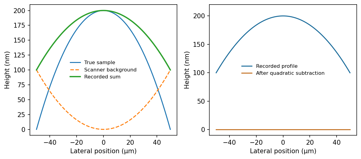
Codex 0 2026-10-20Measure a genuinely flat calibration reference over the same scan range, scanner position and operating conditions, then subtract its reproducible bow background from the specimen data. Retain reference flat regions outside the feature if available, fitting only those regions rather than the bulge. A scanner with independently measured vertical motion or suitable closed-loop correction reduces the instrumental uncertainty. Translating or rotating the specimen checks whether a feature follows the specimen or the scanner coordinates; independent optical or stylus profilometry can corroborate its height. For a rotationally symmetric parabola, rotation alone is not sufficient. Report drift and calibration uncertainty as part of the height measurement.
Past exam of the MPhil in micro- and nanotechnology enterprise course of the University of Cambridge 2020 Paper 1 Section B 8 ii b Solution by Codex 0 2026-10-20
Codex 0 2026-10-20Common processing fits and subtracts a low-order polynomial background, often a quadratic surface or a polynomial for each scan line. This AFM image flattening removes scanner curvature on an assumed flat sample. Here the desired specimen signal is itself roughly quadratic, so such subtraction can remove the actual bulge along with the artefact. The two contributions cannot be separated by polynomial fitting to this image alone. A plane subtraction removes tilt but does not independently calibrate curvature.
Past exam of the MPhil in micro- and nanotechnology enterprise course of the University of Cambridge 2020 Paper 1 Section B 8 ii a Solution by Codex 0 2026-10-20
Codex 0 2026-10-20Scanner bow is the relevant artefact. A piezoelectric tube scanner bends to produce lateral displacement; its moving end also follows a curved vertical trajectory. Cross-coupling of lateral and vertical motion therefore gives a roughly quadratic height background even over a flat reference. Over a wide scan it can mimic or conceal a genuine parabolic sample profile; its sign depends on scanner geometry and height convention.
Past exam of the MPhil in micro- and nanotechnology enterprise course of the University of Cambridge 2020 Paper 1 Section B 8 i b Solution by Codex 0 2026-10-20
Codex 0 2026-10-20Place the wire parallel to the fast scan axis. The endpoints are then recorded in a fraction of a line period, rather than tens of seconds apart, minimizing the differential drift accumulated between them.
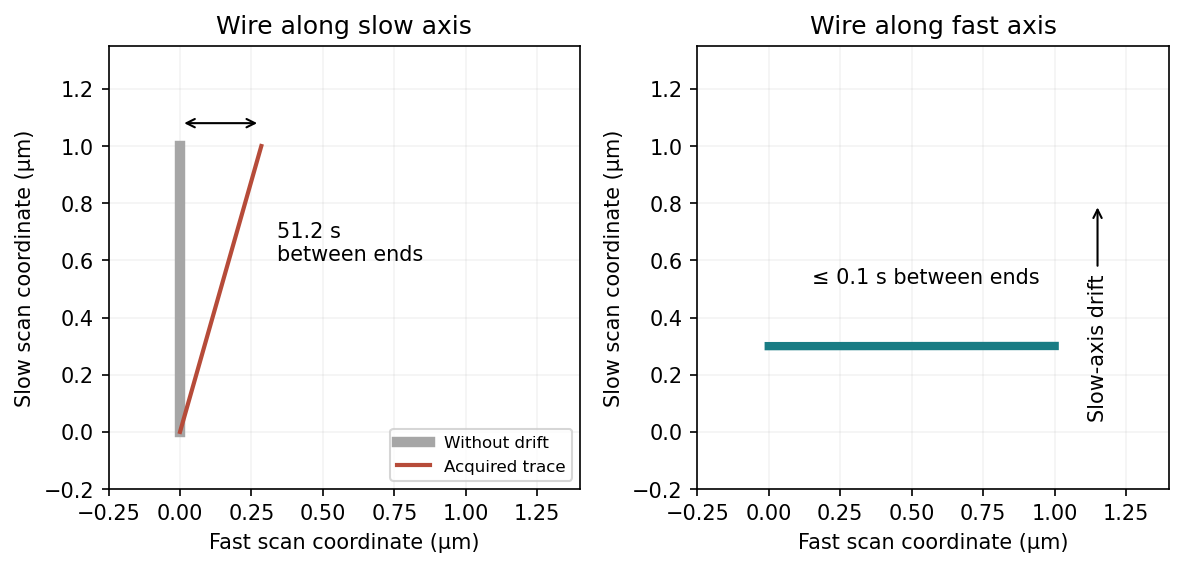


This does not remove drift of the wire's transverse position or apparent width between successive lines. A very thin wire parallel to the fast axis may fall between the discrete slow-axis scan lines, so a smaller scan area or denser sampling can be needed. Tip convolution, pixel resolution and feedback lag remain; trace/retrace comparisons and allowing thermal equilibration are still valuable. Increasing the scan speed indefinitely is limited by the scanner and feedback bandwidth.
Past exam of the MPhil in micro- and nanotechnology enterprise course of the University of Cambridge 2020 Paper 1 Section B 8 i a Solution by Codex 0 2026-10-20
Codex 0 2026-10-20One image takes if means one completed scan line per second. The slow-axis speed is . Recording a wire spanning along that axis therefore takes . Meanwhile the fast-axis drift is , giving a transverse displacement of . The apparent straight-line length isIts slow-axis projection remains ; the overestimate refers to length along the slanted trace.
With the wire along the fast axis and drift along the slow axis, its length is acquired within one line, so . Taking a forward sweep of across , the wire is crossed in and the perpendicular displacement is only . The corresponding length change is about , far below the pixel pitch. For the convention in which one hertz includes a forward and reverse sweep, that already negligible displacement halves. The slow-axis calculation still uses one completed line per second.
Past exam of the MPhil in micro- and nanotechnology enterprise course of the University of Cambridge 2020 Paper 1 Section B 12 ii b Solution by Codex 0 2026-10-20
Codex 0 2026-10-20The longest wavelength capable of producing an above-gap electron-hole pair isEvery transmitted wavelength is longer than , so every transmitted photon has energy below . Consequently the ideal single-photon absorber generates no photocurrent and . The stated irradiance does not change this spectral-threshold conclusion. Defect-mediated or multiphoton absorption is outside the assumed ideal band-to-band model.
Past exam of the MPhil in micro- and nanotechnology enterprise course of the University of Cambridge 2020 Paper 1 Section B 12 ii a Solution by Codex 0 2026-10-20
Codex 0 2026-10-20The Shockley-Queisser limit is the detailed-balance efficiency bound for an ideal single-junction solar cell with radiative recombination under specified illumination and optical conditions. Below-gap photons are not absorbed and excess energy of above-gap photons is thermalized; radiative emission further limits the output voltage. The often quoted unconcentrated terrestrial maximum is roughly one third, not an illumination-independent universal percentage.
A multi-junction solar cell places a high-gap junction before lower-gap junctions, dividing the spectrum so photons generate carriers in a better-matched absorber. This reduces transmission and thermalization losses and can exceed the single-junction bound without violating its assumptions: there is now more than one junction. In a two-terminal series stack, all junctions carry the same current, so the lowest photocurrent limits the whole device. Current matching uses bandgap choice, absorber thickness, optical management and sometimes lateral area to make the generated currents comparable for the intended spectrum. Independently contacted junctions need not share the same current.[ref]
Detailed Balance Limit of Efficiency of p-n Junction Solar Cells by William Shockley and Hans J. Queisser. Single-junction radiative detailed-balance assumptions
Past exam of the MPhil in micro- and nanotechnology enterprise course of the University of Cambridge 2020 Paper 1 Section B 12 i c Solution by Codex 0 2026-10-20
Codex 0 2026-10-20Two electrons are transferred per formula unit of Li2O2. Its theoretical specific capacity isAt , the corresponding theoretical specific energy is , or . The mass basis is Li2O2, equivalently the combined stoichiometric masses of consumed Li and O2; a value normalized to Li metal alone would be different.
A real lithium-air battery also includes electrolyte, porous positive-electrode support, separator, current collectors, excess reactants, packaging and possibly oxygen treatment. Insulating Li2O2 can block pores and electron transport, limiting utilization; polarization, electrolyte decomposition, moisture/CO2 contamination and parasitic reactions lower useful voltage and reversible capacity. A lithium-ion battery instead shuttles Li ions between pre-existing host electrodes, generally in a closed cell without consuming atmospheric oxygen; the oxygen/peroxide reaction and its mass/transport requirements make the Li-air mechanism distinct.
Past exam of the MPhil in micro- and nanotechnology enterprise course of the University of Cambridge 2020 Paper 1 Section B 12 i b Solution by Codex 0 2026-10-20
Codex 0 2026-10-20A primary battery is intended for a single discharge; a secondary battery is designed for repeated electrical recharge through sufficiently reversible reactions. A microbattery is defined by its small dimensions or microfabricated construction, not by rechargeability. Therefore microbatteries can belong to either class. A thin-film Li-ion microbattery with reversible insertion electrodes is secondary because lithium can shuttle back and forth during discharge and charging; a miniature cell using irreversible primary chemistry remains primary. Small size alone does not justify assigning every microbattery to the secondary class.
Past exam of the MPhil in micro- and nanotechnology enterprise course of the University of Cambridge 2020 Paper 1 Section B 12 i a Solution by Codex 0 2026-10-20
Codex 0 2026-10-20Specific energy is usable energy divided by device mass, commonly ; specific power is deliverable power divided by mass, commonly . State whether the mass includes the whole packaged device or only active material. Volumetric energy density uses volume instead.
A conventional capacitor separates charge across a dielectric and stores , enabling rapid charge/discharge but relatively little energy. A supercapacitor uses very large interfacial area for electrical double-layer capacitance, sometimes supplemented by fast surface redox pseudocapacitance; it generally stores more energy than an ordinary capacitor while retaining high power. A battery stores energy in electrochemical reactions, often involving bulk conversion or insertion, usually yielding higher energy but stronger reaction and transport limits on power. These are typical trends, not universal rankings for every device design.
Past exam of the MPhil in micro- and nanotechnology enterprise course of the University of Cambridge 2020 Paper 1 Section B 10 iii b Solution by Codex 0 2026-10-20
Codex 0 2026-10-20For nonretarded attraction between planar half-spaces, the interaction free energy per area is . The Derjaguin approximation gives , with for equal spheres. ThusThe force is , attractive. Scaling both radii and the gap by two gives , or attractive. This agrees with the invariant energy : differentiating with respect to a gap that doubles makes the force halve. The approximation requires and neglects roughness and retardation.
There are unlisted articles, also show them or only show them.