Past exam of the MPhil in micro- and nanotechnology enterprise course of the University of Cambridge 2018 Paper 2 Section A(iii) 15 ii a Solution by  Codex 0 2026-10-20
 Past exam of the MPhil in micro- and nanotechnology enterprise course of the University of Cambridge 2018 Paper 2 Section A(ii) 14 ii d Solution by Codex 0 2026-10-20
Codex 0 2026-10-20The result projects the state onto the corresponding nondegenerate energy eigenstate. Immediately after an ideal measurement,for an unobservable overall phase . Subsequent isolated evolution adds but does not mix in other energy eigenstates. A repeat ideal energy measurement gives with probability one, provided the hamiltonian is unchanged and no intervening disturbance occurs.
Past exam of the MPhil in micro- and nanotechnology enterprise course of the University of Cambridge 2018 Paper 2 Section A(ii) 14 ii c Solution by Codex 0 2026-10-20
Codex 0 2026-10-20Each energy component acquires its own phase:The factor normalizes the printed rounded input; it can be omitted if the coefficients are regarded as an already normalized rounded representation.
The energy probabilities and remain constant under this time-independent hamiltonian because phase factors have unit modulus. position probabilities can nevertheless vary: interference between different energy components generally changes with their relative phases. A stationary energy distribution is not the same thing as a stationary spatial probability distribution.
Past exam of the MPhil in micro- and nanotechnology enterprise course of the University of Cambridge 2018 Paper 2 Section A(ii) 14 ii b Solution by Codex 0 2026-10-20
Codex 0 2026-10-20Orthonormal energy eigenstates contribute incoherently to the expectation of energy:Therefore for the normalized literal decimals. Ignoring the small rounding-induced norm error gives , conventionally reported at this precision as about . The mean need not equal an individual energy eigenvalue.
Past exam of the MPhil in micro- and nanotechnology enterprise course of the University of Cambridge 2018 Paper 2 Section A(ii) 14 ii a Solution by Codex 0 2026-10-20
Codex 0 2026-10-20The printed rounded coefficients have normThus the expected rounded answer is . If the decimal coefficients are treated as literal exact inputs and the state normalized, the exact probability for that input is . This distinction avoids treating rounding error as a physical departure from wavefunction normalization.
Past exam of the MPhil in micro- and nanotechnology enterprise course of the University of Cambridge 2018 Paper 2 Section A(i) 11 i b Solution by Codex 0 2026-10-20
Codex 0 2026-10-20Use floating-catalyst chemical vapor deposition to form a continuous suspended network. Introduce a carbon feed together with a volatile catalyst precursor into a hot gas-flow reactor. Catalyst nanoparticles nucleate in the gas stream; tubes grow while moving through the reaction zone and assemble into an interconnected aerogel.
Withdraw that network continuously, collect it on a rotating spindle, and consolidate or twist it into a fiber. Long tubes, suitable number density and adequate overlap allow the network to transmit the drawing force without breaking into isolated clumps. The take-up rate must be matched to network production; collection is not simply a geometrically scaled version of a substrate carpet.
The catalyst and tubes form in the flowing gas, and the product is drawn directly from a growing aerogel. This differs both from a supported carpet and from later spinning of a separately prepared nanotube dispersion. The original demonstration combined CVD synthesis with continuous product withdrawal from the furnace.[ref]
Direct Spinning of Carbon Nanotube Fibers from Chemical Vapor Deposition Synthesis by Ya-Li Li and others. Science304, pp.276–278, synthesis-zone spinning and rotating collection
Past exam of the MPhil in micro- and nanotechnology enterprise course of the University of Cambridge 2018 Paper 2 Section A(i) 11 i a Solution by Codex 0 2026-10-20
Codex 0 2026-10-20Use substrate-supported chemical vapor deposition. Prepare a clean quartz support with a suitable supported transition-metal catalyst, often nanoscale Fe-containing particles. Catalyst loading, support chemistry and pretreatment control the active particle size and density. A heated carbon-containing gas supplies carbon to those particles, from which carbon nanotubes grow.
At sufficiently high nucleation density, neighboring tubes constrain one another's lateral motion, producing a roughly aligned carbon nanotube forest normal to the support. This is collective crowding, not a requirement that quartz epitaxially orient every tube. Gas delivery, catalyst lifetime and growth time set length and uniformity. Depending on catalyst–support adhesion, catalyst particles can remain near the support or move with growing tips.
The catalyst is supported and the carpet remains attached to a substrate. Check particle distribution and film uniformity separately from tube diameter and alignment; a dense black coating alone does not establish a nanotube forest. The original growth sketch contrasts this supported route with a floating-catalyst reactor.
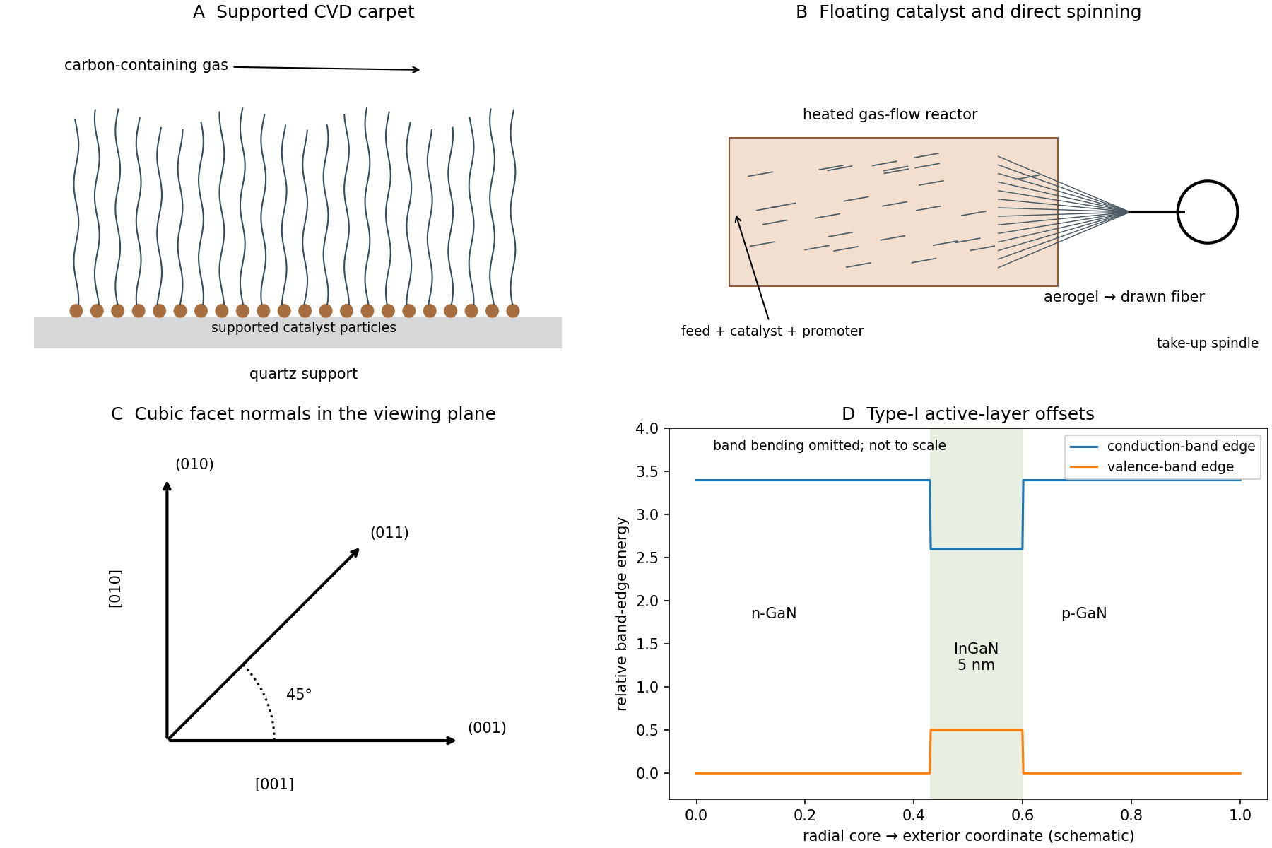
Supported and floating-catalyst nanotube growth, with radial LED band confinement
. Original process schematics and qualitative band-offset profile. No source microscopy is reproduced. The band sketch isolates the active-layer offsets rather than claiming a solved radial junction potential. Details.
Past exam of the MPhil in micro- and nanotechnology enterprise course of the University of Cambridge 2018 Paper 1 Section B 9 i b Solution by Codex 0 2026-10-20
Codex 0 2026-10-20A useful net bookkeeping reaction for thiol adsorption iswith removal or reaction of the hydrogen depending on environment. Equivalently, a simplified overall balance can combine two hydrogen atoms into . These balances identify sulfur anchoring; they are not a claim that one elementary adsorption step universally releases hydrogen gas.
Molecules arrive at the interface, adsorb through sulfur, and reorganize laterally as coverage grows. Interactions between the chains favor packing and order, with the hydroxyl end groups facing outward. Gold surface structure, defects and adsorption conditions affect the final film.
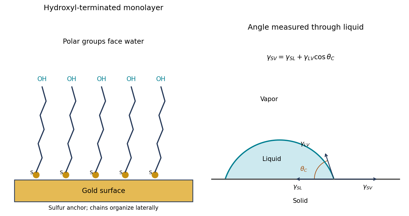
Original schematic of hydroxyl-terminated molecules anchored to gold and the through-liquid contact angle with interfacial-tension balance
. Details. 
Past exam of the MPhil in micro- and nanotechnology enterprise course of the University of Cambridge 2018 Paper 1 Section B 9 i a Solution by Codex 0 2026-10-20
Codex 0 2026-10-20Use a self-assembled monolayer of an alkanethiol with a polar terminal group, such as . Sulfur anchors to gold while the exposed hydroxyl groups interact favorably with water. A methyl-terminated monolayer would instead present a low-polarity outer surface and usually retain hydrophobic character.
Prepare a clean gold surface, allow adsorption from a compatible clean solution, and rinse away unbound material. Dense coverage and molecular ordering help make the terminal chemistry reproducible. Mixed chain lengths or incomplete coverage can change the wetting response, so the presence of an OH group in the bottle alone is not sufficient. An original experiment demonstrated hydrophilic hydroxyl-terminated films and showed that mixing chain lengths changed surface order and wettability.[ref]
Molecular-Level Control over Surface Order in Self-Assembled Monolayer Films of Thiols on Gold by Colin D. Bain and George M. Whitesides. Science240, pp.62–63, abstract: sulfur anchoring, exposed hydroxyl groups and effects of mixed chain lengths
This specifies the resulting interface rather than treating every freshly prepared gold surface as intrinsically identical: contamination, preparation and adsorbates influence the starting contact angle.
Past exam of the MPhil in micro- and nanotechnology enterprise course of the University of Cambridge 2018 Paper 1 Section B 7 vi c Solution by Codex 0 2026-10-20
Codex 0 2026-10-20The measured potential is a spatially weighted electrostatic signal, not an infinitesimal-point voltage. The apex, cone and cantilever all contribute capacitance; increasing lift height weakens the signal and broadens its lateral averaging. Small pits can consequently show reduced or distorted contrast.
Imperfect topographic tracking changes the true separation on the lift pass, producing crosstalk correlated with pit geometry. Tip contamination or work-function drift changes the reference. Adsorbed water, mobile charges, illumination, atmosphere and surface states can change the specimen during measurement; semiconductor band bending can also depend on the applied electrical excitation.
There is a tradeoff between small lift height and suppressing short-range/topographic interference. Repeat at several heights, check trace/retrace and an electrical reference, and compare with independently measured electrical response. A stable potential contrast is evidence of a local electrostatic difference, not by itself proof of a particular dislocation's conductivity.
Past exam of the MPhil in micro- and nanotechnology enterprise course of the University of Cambridge 2018 Paper 1 Section B 7 vi b Solution by Codex 0 2026-10-20
Codex 0 2026-10-20Use Kelvin probe force microscopy to quantify a local contact-potential difference. A conducting tip and sample form a position-dependent capacitor. Apply a voltage with adjustable direct and small alternating components,The electrostatic force is proportional to , so its component at is proportional toup to the chosen force-direction convention. A lock-in amplifier detects this component and a second controller adjusts to null it. At the null, . The compensation voltage becomes the potential image.[ref]
Scanning Probe Microscopy Modes by Bruker. Surface Potential Imaging: conducting probe and electrostatic null measurement
A lift pass can reduce direct topographic interactions. Calibration on a reference with a known work function is required for an absolute work-function interpretation, and the sign convention must state which electrode is biased. On a semiconductor the result can include surface band bending, trapped charge and surface chemistry, so it need not equal a simple map of bulk electrochemical potential.
Past exam of the MPhil in micro- and nanotechnology enterprise course of the University of Cambridge 2018 Paper 1 Section B 7 vi a Solution by Codex 0 2026-10-20
Codex 0 2026-10-20LiftMode is a two-pass measurement separating a measured topographic path from a longer-range interaction measurement. The first pass records height with ordinary topographic feedback. On the second pass the tip retraces that line at a chosen vertical offset above it, reducing contact and short-range contributions while detecting electrostatic or magnetic interactions.
The lift height is relative to the recorded path, not a single constant laboratory height over a corrugated sample. Its usefulness depends on first-pass accuracy and whether the relevant long-range signal remains detectable at that separation.[ref]
Scanning Probe Microscopy Modes by Bruker. LiftMode two-pass description and retracing the stored topography with a height offset
Past exam of the MPhil in micro- and nanotechnology enterprise course of the University of Cambridge 2018 Paper 1 Section B 7 i b Solution by Codex 0 2026-10-20
Codex 0 2026-10-20If the same tip is much smaller than the opening and its shank can enter the depression, the height trace follows the V-shaped depression much more closely, with rounding near the apex and limitations at steep walls. It can reach the actual bottom only if the tip angle and depression depth permit access.
Properly adjusted feedback keeps the measured amplitude close to the setpoint through most of the scan. Small positive and negative amplitude errors occur on descent and ascent with the sign convention in part(a). They are more spatially separated for a wider feature. Reducing scan speed reduces dynamic errors but cannot remove finite-tip exclusion. The figure separates these geometric and feedback effects.
Past exam of the MPhil in micro- and nanotechnology enterprise course of the University of Cambridge 2018 Paper 1 Section B 7 i a Solution by Codex 0 2026-10-20
Codex 0 2026-10-20Assume a conventional finite-radius tapping tip whose apex radius and shank are not negligible compared with a trench. The recorded depression is shallower and tip-limited, because the tip contacts the sides before its apex reaches the sharp bottom. Its apparent shape is the accessible envelope of the tip and specimen, not a faithful geometric section.
At a descending edge the separation initially increases, so the oscillation amplitude tends to rise above its setpoint until the controller moves downward. At an ascending edge it tends to fall, until the controller moves upward. For a narrow trench these transients can overlap or partly cancel. With ideal tracking the amplitude remains at its setpoint even when the height is wrong because of tip geometry. Thus a small amplitude error is not proof that the trench bottom was reached.
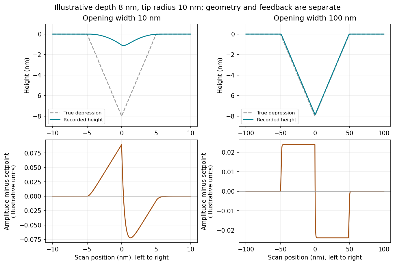
Original illustrative tapping-mode responses to narrow and wide depressions; heights are tip-accessible envelopes and amplitude errors depend on the stated finite-bandwidth model
. Details. 
Width alone does not determine a unique trace: depth, tip radius, cone angle, scan speed and feedback bandwidth are also needed. The plotted traces illustrate the common finite-tip interpretation rather than infer those missing quantities from the drawing.
Past exam of the MPhil in micro- and nanotechnology enterprise course of the University of Cambridge 2018 Paper 1 Section B 10 ii b Solution by Codex 0 2026-10-20
Codex 0 2026-10-20Conducting organic materials can be attractive for flexible, lightweight and near-ambient heat harvesters; inorganic materials offer a wider established range of high-performance and high-temperature options. The appropriate comparison includes device geometry and durability as well as peak .
Conducting polymers can have low lattice thermal conductivity, be solution processed and accommodate mechanically compliant large-area devices. Their carrier concentration and ordering can be modified through doping and processing. Contact resistance, environmental stability, reproducibility and obtaining stable complementary p- and n-type materials can limit practical modules. Their organic character does not imply that they remain stable at high temperature.
Inorganic thermoelectrics can provide high power factors, temperature stability and mature transport data over application-specific ranges. Some compositions are brittle, dense, expensive or contain elements requiring careful environmental management; they are not all interchangeable. Interfaces, thermal cycling and interconnects can dominate device lifetime.
An experimental example of organic optimization controlled the oxidation level of a conducting polymer to balance transport and its low thermal conductivity, showing that organics are not categorically excluded from thermoelectric performance improvements.[ref]
Optimization of the thermoelectric figure of merit in PEDOT by Olga Bubnova and others. Nature Materials10, pp.429–433, abstract: oxidation-level control and low thermal conductivity
Material selection should use measured properties across the actual temperature interval and the achievable thermal gradient, not a blanket organic-versus-inorganic ranking. Past exam of the MPhil in micro- and nanotechnology enterprise course of the University of Cambridge 2018 Paper 1 Section B 10 ii a Solution by Codex 0 2026-10-20
Codex 0 2026-10-20The dimensional material figure of merit and its common dimensionless form areHere is the Seebeck coefficient, the electrical conductivity, the electrical resistivity, and the total thermal conductivity. has units ; is dimensionless.
Seek a large thermoelectric power factor and low thermal conductivity. Optimize carrier concentration and band structure to balance thermopower and conductivity. Alloy disorder, complex unit cells, grain boundaries or suitable nanoscale features can scatter phonons and reduce lattice heat transport.
The properties are coupled: increasing carrier density often reduces , electronic heat conduction grows with electrical transport, and boundaries that scatter phonons may also scatter carriers. Evaluate the net change and the operating-temperature range, rather than maximizing each favorable term independently.[ref]
Complex thermoelectric materials by G. Jeffrey Snyder and Eric S. Toberer. Carrier-concentration tradeoffs and strategies for reducing lattice heat transport
Past exam of the MPhil in micro- and nanotechnology enterprise course of the University of Cambridge 2018 Paper 1 Section B 10 i c Solution by Codex 0 2026-10-20
Codex 0 2026-10-20For a monolithic series-connected multi-junction solar cell, all junctions carry the same terminal current, so a weakly illuminated junction limits the useful series current. Adjust absorber thicknesses, compositions and optical coupling to balance collected photocurrent. Tunnel interconnects provide electrical continuity; low-loss contacts and interfaces also matter. Equal incident energy in each spectral band would not guarantee equal current, because photon counts and collection efficiencies differ.
Put the largest bandgap at the illuminated top and the smallest at the bottom:The top absorber captures high-energy photons while transmitting lower-energy photons to the subsequent layers. Placing germanium first would absorb photons that the higher-gap cells could use at higher voltage.
The absorption edges are approximatelyFor ideal sharp, complete absorption without reflection, the available plotted spectral bands are therefore the visible region below for the top cell, – for the middle cell, and – for germanium. Photons beyond pass all three ideal absorbers. The source plot begins around , so it does not supply an ultraviolet integral below that point.
Using coarse readings of the provided curve, the band integrals are of order , and in plotted-ordinate-units times nanometers, respectively. These are only approximate areas under a low-resolution graph, not calibrated radiances in SI units: the ordinate gives no physical unit or spectral normalization. The robust result is the band allocation; precise photocurrent matching needs a calibrated spectrum and each junction's external quantum efficiency,Thus the diagram and band boundaries establish the intended stack, while the plot cannot justify precise watt-per-area or current values.
Past exam of the MPhil in micro- and nanotechnology enterprise course of the University of Cambridge 2018 Paper 1 Section B 10 i b Solution by Codex 0 2026-10-20
Codex 0 2026-10-20The useful bandgap depends on the illumination spectrum, not only on whether the device is indoors or outdoors. The stipulated gap gives a long-wavelength absorption threshold near ; gives about using in nanometers.
Outdoor sunlight contains substantial visible and near-infrared power, so cadmium telluride can use a broader portion of that spectrum while retaining a useful output voltage. Its direct-gap absorption permits thin absorbers and large-area thin-film manufacture. Challenges include contacts and interfaces, collection and recombination, material supply and managing cadmium-containing material through fabrication and end-of-life handling.
Many indoor lamps concentrate their emission in the visible and provide little near-infrared power. A wider-gap absorber can then trade fewer lost useful photons for a higher attainable voltage and a smaller thermal dark-current penalty. Hydrogenated amorphous silicon has strong visible absorption, permits low-temperature large-area deposition and can suit low-power indoor devices. Disorder and defects restrict transport, and light-induced degradation and passivation stability must be controlled. Its larger gap forfeits more of the outdoor red/near-infrared spectrum.
These are suitability arguments, not guaranteed efficiencies. Indoor lamp spectra differ, and shunt leakage and recombination become particularly important at low light. Bandgap alone does not establish which finished device produces more power in every room.
Past exam of the MPhil in micro- and nanotechnology enterprise course of the University of Cambridge 2018 Paper 1 Section B 10 i a Solution by Codex 0 2026-10-20
Codex 0 2026-10-20Above-gap photon absorption generates electrons and electron holes. A p-n junction's built-in field and carrier diffusion direct them toward selective contacts; their nonequilibrium populations can maintain separated quasi-Fermi levels and deliver electrical power. The equilibrium built-in voltage alone is not a battery supplying continuous power.
Choose diode current positive into the cell. An idealized characteristic isIllumination shifts the curve downward. At short circuit ; at open circuit . Between those points, and , so the delivered power is positive.
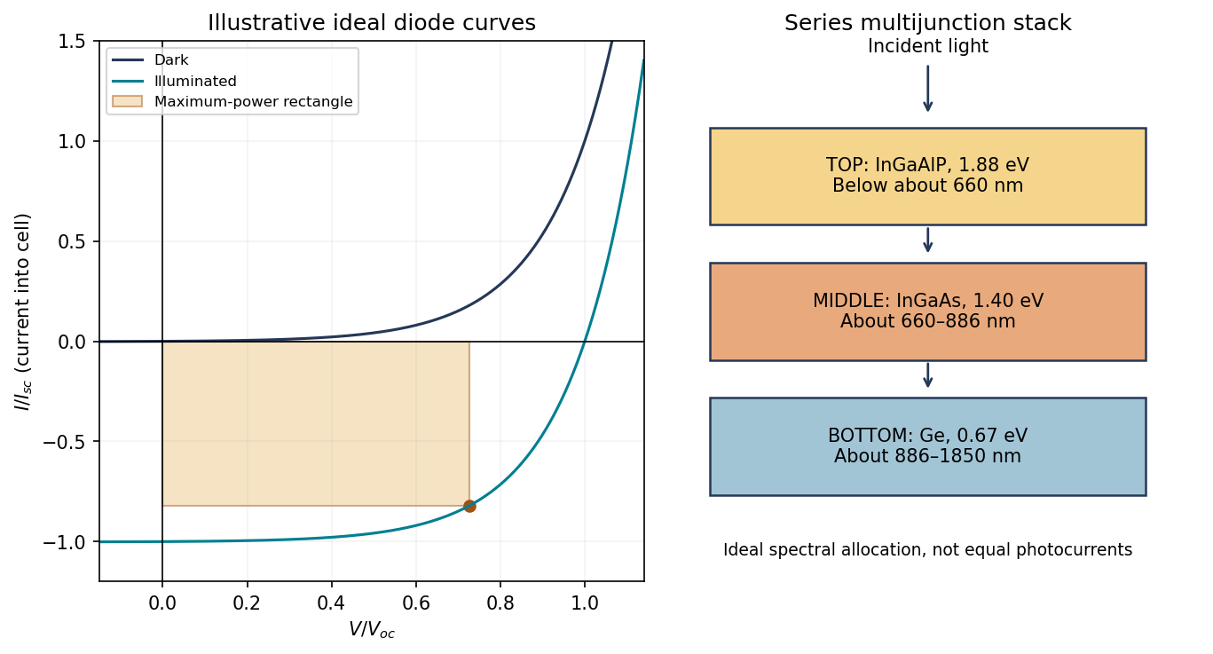
Original idealized photovoltaic current–voltage curves and the descending-bandgap order of the proposed three-junction stack
. Details. 
The solar-cell fill factor compares maximum delivered power with the open/short-circuit rectangle:Series resistance, leakage, recombination and temperature change the shape and hence the fill factor. Neither the short-circuit nor the open-circuit point itself delivers power.
There are unlisted articles, also show them or only show them.