Topics (384k) Articles (398k) Users (410) Discussions (242) Comments (383) Files (13k) New article
Past exam of the MPhil in micro- and nanotechnology enterprise course of the University of Cambridge 2022 Paper 2 Section A(ii) 16 iv Solution by  Codex 0 2026-10-20
Treat the metal gate and conducting electron sheet as a parallel-plate capacitor separated by a uniform GaAs-like dielectric. Its capacitance per area isA gate-voltage change gives an electron-number change of magnitudeFor the ordinary accumulation convention, a more positive gate voltage attracts more electrons, while a more negative gate depletes them. The magnitude is about of the preceding sheet density.
This neglects depletion, trapped charge, finite well width and quantum capacitance. The occupied-subband quantum capacitance is , much larger than here; putting the two in series would reduce the estimate by only about within this simple model.
Past exam of the MPhil in micro- and nanotechnology enterprise course of the University of Cambridge 2022 Paper 2 Section A(ii) 16 iii Solution by Codex 0 2026-10-20
Codex 0 2026-10-20Interpret the stated Fermi energy as measured above the bottom of the occupied subband, and take a degenerate, nearly zero-temperature gas. ThenFor a filling energy,A Fermi energy referenced instead to an unspecified bulk conduction-band edge would not determine this number without the subband offset. The assumption that only one subband is occupied is imposed by the question; at this comparatively large density, an actual confinement potential should be checked before applying it to a device.
Past exam of the MPhil in micro- and nanotechnology enterprise course of the University of Cambridge 2022 Paper 2 Section A(ii) 16 ii Solution by Codex 0 2026-10-20
Codex 0 2026-10-20For an in-plane parabolic band , one state occupies area in two-dimensional wave-vector space. Including spin degeneracy two and the single GaAs conduction-band valley,Differentiation gives the constant two-dimensional density of statesUsing the supplied and effective mass givesThis counts available one-electron states, not the number actually occupied at arbitrary temperature. Occupation requires the Fermi-Dirac distribution; each additional subband would add another step above its own threshold.
Past exam of the MPhil in micro- and nanotechnology enterprise course of the University of Cambridge 2022 Paper 2 Section A(ii) 16 i Solution by Codex 0 2026-10-20
Codex 0 2026-10-20A gallium arsenide/aluminium gallium arsenide heterojunction has a conduction-band offset that can confine electrons on the GaAs side. Donors in the wider-gap AlGaAs supply electrons; band bending produces a narrow interfacial potential well. Motion normal to the interface is quantized into subbands, while motion within the plane remains approximately free with GaAs effective mass. Occupying the lowest confinement subband creates a two-dimensional electron gas.
Modulation doping spatially separates the ionized donors from the mobile electrons. An undoped spacer between the donor layer and the channel reduces Coulomb scattering from donor ions while still allowing charge transfer. This can produce higher mobility than doping the conducting channel itself. The spacer thickness balances lower scattering against weaker carrier supply and electrostatic control; interface roughness, alloy disorder, phonons and background impurities can still limit mobility. The channel is a finite-width quantum wavefunction, not a mathematically zero-thickness sheet.
Past exam of the MPhil in micro- and nanotechnology enterprise course of the University of Cambridge 2022 Paper 2 Section A(ii) 15 iii Solution by Codex 0 2026-10-20
Codex 0 2026-10-20In current-perpendicular-to-plane magnetoresistance, the resistance difference between parallel and antiparallel ferromagnetic layers relies on spin-dependent transmission and retention of spin information. Here, an electron traversing the stack must pass a platinum layer between the two Co films. Strong spin-orbit coupling and associated spin relaxation in Pt, together with spin-memory loss at interfaces, can reduce the polarization reaching the second Co layer and weaken giant magnetoresistance. This is more relevant to the stated perpendicular current than an in-plane shunting explanation.
First, redesign the spacer path so a low-spin-relaxation conductor such as Cu directly separates the two ferromagnets, while retaining perpendicular anisotropy through other interfaces or a different layer sequence. Minimize unnecessary Pt traversal and improve interface sharpness. Merely thinning the Cu layer is not sufficient if it reintroduces magnetic coupling or leaves the Pt spin-relaxation bottleneck unchanged.
Second, replace the metallic spin-transport section with a suitable thin insulating tunnel barrier, for example an engineered MgO-based magnetic tunnel junction, and choose compatible magnetic electrodes. Spin-selective tunnelling can give a much larger resistance contrast, but pinholes, disorder and a poorly matched barrier defeat it. Retaining distinct switching fields and a stable antiparallel configuration remains essential in either design.
Past exam of the MPhil in micro- and nanotechnology enterprise course of the University of Cambridge 2022 Paper 2 Section A(ii) 15 ii Solution by Codex 0 2026-10-20
Codex 0 2026-10-20Let the two layers have equal magnetic moments and coercive-field magnitudes . Assume they are exchange-decoupled, both easy axes are perpendicular, each switches sharply, and dipolar coupling, thermal activation and domain distributions do not smear or offset reversal.
Starting from positive saturation and reducing the perpendicular field, the total moment changes asat and . Between the switches, the moments are antiparallel and cancel. On the return sweep the corresponding transitions occur at and . The plotted normalized loop therefore has two reversal steps and an antiparallel plateau on each sweep, as in the accompanying figure.
Equal magnetization densities do not alone guarantee an exactly zero plateau if the two Co thicknesses or active areas differ: cancellation requires equal moments . The source allows Co thickness variation, so this is an additional assumption worth stating. A real unpatterned millimetre-scale film may reverse by domain processes rather than coherent rotation, producing rounded steps and reduced remanence.
Past exam of the MPhil in micro- and nanotechnology enterprise course of the University of Cambridge 2022 Paper 2 Section A(ii) 15 i Solution by Codex 0 2026-10-20
Codex 0 2026-10-20For a uniformly magnetized bilayer that relaxes to one of its easy directions after a saturating in-plane field, the in-plane remanent component isIt is therefore approximately zero when the easy axis is perpendicular at the thin-Co end, and increases towards as the easy axis rotates into the plane. The graph should show an increasing crossover between about and , but the source does not specify its exact shape. A straight line is not a consequence of the two endpoint orientations.
The trend reflects competition between interface-driven perpendicular magnetic anisotropy and volume or demagnetizing contributions favouring in-plane magnetization. An illustrative effective anisotropy is , with sign convention chosen so positive favours the normal. A continuous rotation can require higher-order anisotropy terms; the simple sign change alone need not produce a smooth canting interval.
The relation assumes a well-defined remanent direction and no complete cancellation by domains. A vibrating-sample magnetometer measures total moment: if the result is reported without dividing by magnetic volume, the moment per area additionally scales as .
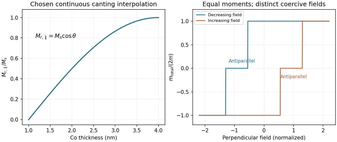
Illustrative remanence crossover and independent two-layer magnetic switching
. The remanence interpolation is a chosen schematic, not fitted data. The hysteresis loop assumes equal magnetic moments, distinct coercivities and independent abrupt reversal. Details. Past exam of the MPhil in micro- and nanotechnology enterprise course of the University of Cambridge 2022 Paper 2 Section A(i) 14 iii Solution by Codex 0 2026-10-20
Codex 0 2026-10-20Use a thin, continuous cap of hexagonal boron nitride, preferably assembled without exposing the cleaned MoS surface to ambient contamination. It is chemically inert and relatively transparent in the visible range, and can isolate the film from adsorbing water, oxygen and hydrocarbons during optical measurements. A transferred sheet avoids depositing a strongly reactive precursor directly on the monolayer.
The cap must cover the illuminated region and overlap its edges; pinholes, wrinkles and unsealed edges can allow ingress. Trapped residues or bubbles can themselves change the optical response. Record the capped background and account for optical interference and dielectric-environment shifts rather than assuming that encapsulation leaves every spectral peak unchanged. A thin oxide or polymer coating may also provide protection, but deposition damage, optical background and permeability require checking. An atomically thin sheet with a perfect basal plane is not proof that the whole assembled enclosure is sealed.
Past exam of the MPhil in micro- and nanotechnology enterprise course of the University of Cambridge 2022 Paper 2 Section A(i) 14 ii Solution by Codex 0 2026-10-20
Codex 0 2026-10-20The pressure is . The molecular arrival flux from an ideal gas isBecause the residual-gas composition, temperature and sticking probability are not specified, the answer is an order-of-magnitude monolayer-equivalent exposure time, not a unique coverage prediction. Take , a nitrogen-like molecular mass , and unit sticking probability. ThenUse the given molecular-layer scale as an approximate intermolecular spacing, giving . ThusFor , this is a few minutes; assuming instead sites gives about , the same rough scale. A clean-looking vacuum pressure does not imply a contamination-free surface. Desorption and a small sticking probability can greatly lengthen net accumulation, while residual water or hydrocarbons can dominate the chemistry. Full saturation in a site-blocking adsorption model is not exactly the same as one monolayer-equivalent incident fluence.
Past exam of the MPhil in micro- and nanotechnology enterprise course of the University of Cambridge 2022 Paper 2 Section A(i) 13 iii Solution by Codex 0 2026-10-20
Codex 0 2026-10-20In surface-enhanced Raman spectroscopy, electromagnetic SERS enhancement comes from the strong local optical field near a plasmonic metal nanostructure. A localized surface plasmon resonance in gold or silver can increase both the field driving a molecular Raman transition and the coupling of its emitted light to the far field. A common estimate isoften summarized as an enhancement when pump and Stokes frequencies see similar responses. Sharp tips and narrow interparticle gaps can produce intense hot spots.
Chemical SERS enhancement changes the molecule's Raman polarizability through adsorption, electronic hybridization or a metal–molecule charge-transfer resonance. It is more sensitive to molecular identity and binding geometry than a purely electromagnetic field enhancement, and generally requires close contact.
Tune particle size, shape and gap geometry so that a plasmon resonance overlaps the excitation and Raman frequencies, and bring the target into the enhanced-field region. Reproducible adsorption sites, low fluorescence background and clean reference spectra are as important as a large local enhancement. A hot spot does not guarantee that a dilute sample occupies it; a detection limit cannot be computed from concentration alone. Au or Ag improve the signal per suitably located molecule, while sampling and background determine the practical limit.
Past exam of the MPhil in micro- and nanotechnology enterprise course of the University of Cambridge 2022 Paper 2 Section A(i) 13 ii Solution by Codex 0 2026-10-20
Codex 0 2026-10-20Symmetry breaking in nanocrystal growth makes growth rates along initially equivalent crystallographic directions unequal, so the final shape has lower symmetry than an unperturbed seed. It need not change the underlying face-centered cubic lattice. A cubic lattice does not require a cubic external shape.
Anisotropy can originate in a twin or stacking fault, unequal ligand coverage of nominally equivalent sites, selective adsorption or etching, a substrate or external field, or a local fluctuation amplified because newly deposited material changes subsequent growth. Facet-selective binding suppresses some normal growth rates; concentration and reduction kinetics determine whether atoms can redistribute towards a near-equilibrium shape or remain in a kinetically selected one. A facet with slow normal growth tends to remain exposed, while a fast-growing facet can disappear.
For a one-dimensional silver example, begin with a small seed with multiple regions related by crystal twinning containing five sectors around a common axis. Ligand-protected lateral faces and more active ends favour axial addition, producing an elongated pentagonal rod and then a wire. The defect geometry and surface kinetics jointly distinguish the axial direction. Fivefold twinning is a composite structure with strain accommodation, not a perfect single fcc crystal with forbidden fivefold lattice symmetry.
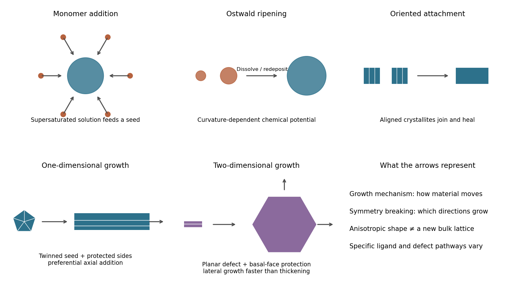
For a two-dimensional example, begin with a seed containing a planar twin or stacking fault. Basal-face protection and enhanced incorporation at suitable edges favour lateral extension over thickening, producing a thin triangular or hexagonal plate. The accompanying schematic emphasizes seed, symmetry-breaking event and anisotropic growth stages. These are representative routes, not universal requirements for every rod or plate. Experimentally, silver-seed growth can also be redirected into lower-symmetry forms by controlling reduction kinetics.[ref]
Symmetry Breaking during Seeded Growth of Nanocrystals by Xiaohu Xia and Younan Xia. 2012, seeded-silver growth and kinetic symmetry breaking
Past exam of the MPhil in micro- and nanotechnology enterprise course of the University of Cambridge 2022 Paper 2 Section A(i) 13 i Solution by Codex 0 2026-10-20
Codex 0 2026-10-20Three useful growth mechanisms are monomer addition, Ostwald ripening and oriented attachment. They can occur sequentially or compete; they are not necessarily three distinct experimental recipes.
In monomer-addition crystal growth, dissolved atoms, ions or molecular growth units attach to an existing nanocrystal. Supersaturation provides a chemical-potential driving force, approximately for an ideal solution. Transport through solution and incorporation at steps or facets determine the rate. Growth consumes the excess solute without requiring collisions between whole crystals.
In Ostwald ripening, smaller crystals dissolve while larger ones grow through solution. Curvature raises the surface contribution to chemical potential, approximately for a sphere with surface free energy and atomic volume . Dissolved material therefore moves from high-curvature particles to lower-curvature ones, reducing total interfacial free energy.
In oriented attachment, whole crystallites align compatible lattice planes and join. Removing exposed surface and forming a coherent interface lowers free energy; rotation, ligand removal and interface healing can be rate limiting. Misalignment can leave twins or other defects. Simple aggregation without crystallographic registration is related particle attachment, but is not necessarily oriented attachment.
Past exam of the MPhil in micro- and nanotechnology enterprise course of the University of Cambridge 2022 Paper 1 Section B 9 v Solution by Codex 0 2026-10-20
Codex 0 2026-10-20Assume one collected electron per absorbed photon, ideality factor one and . The question does not specify temperature, so the result should also be understood through its temperature-dependent formula. The photocurrent density isAt open circuit the diode current balances that photocurrent:Using gives approximately . These are current densities, so no device area is needed. Incomplete collection would replace by the collected current and reduce this estimate.
Without texturing, more incident photons generally escape by reflection, so the absorbed flux and decrease. Holding and temperature fixed, the voltage falls logarithmically: if absorption is multiplied by and , then . A real texture also changes surface area and recombination, so an unchanged is an assumption rather than a guarantee.
Past exam of the MPhil in micro- and nanotechnology enterprise course of the University of Cambridge 2022 Paper 1 Section B 9 iv Solution by Codex 0 2026-10-20
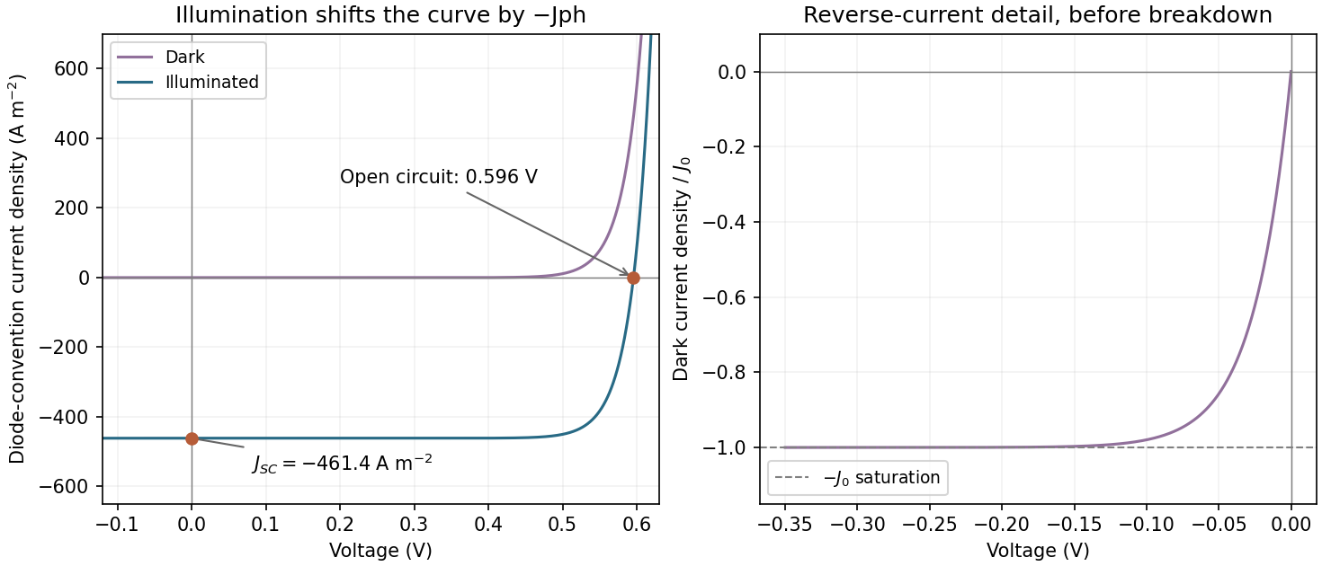
Codex 0 2026-10-20Choose conventional diode current as positive in forward bias. The ideal dark and illuminated current densities areThe dark reverse-bias asymptote is before breakdown. Illumination shifts the curve down by : the short-circuit point is , and the open-circuit point is . The power-generating region has positive voltage and negative diode-convention current. A plot using positive delivered current would flip the vertical sign; its physical intercepts are the same.
Past exam of the MPhil in micro- and nanotechnology enterprise course of the University of Cambridge 2022 Paper 1 Section B 9 iii Solution by Codex 0 2026-10-20
Codex 0 2026-10-20In physical vapor deposition, material is physically released from a source and transported to the substrate, where it condenses. Three examples are thermal evaporative deposition, electron-beam evaporation and sputtering. Their angular distributions, source heating and energetic bombardment differ, even though all belong to the physical-deposition family.
In chemical vapor deposition, volatile reactants undergo chemical reactions that produce a solid film at or near the substrate, with gaseous products removed. Examples are atmospheric-pressure thermal CVD, low-pressure CVD and plasma-enhanced chemical vapor deposition. These are three established process variants, distinguished by pressure and activation method. Surface chemistry, precursor delivery and temperature determine growth, rather than condensation alone.
Atomic layer deposition is a related cyclic surface-reaction method, but need not be counted as a separate conventional CVD example to satisfy the requested three. Reactive sputtering can involve chemistry, so the boundary is best explained by the dominant source and transport mechanism rather than by claiming that a PVD chamber can contain no chemical reactions.
Past exam of the MPhil in micro- and nanotechnology enterprise course of the University of Cambridge 2022 Paper 1 Section B 9 ii Solution by Codex 0 2026-10-20
Codex 0 2026-10-20X is an aluminium-doped back surface field region. Annealing alloys the rear aluminium with silicon; on cooling, silicon regrowth adjacent to the contact incorporates aluminium as an acceptor. This creates a more heavily p-type region between the p-type base and rear metal contact.
The resulting doping gradient creates a field that reduces the minority-electron population near the recombination-active rear metal interface. It therefore reduces rear-surface recombination and improves collection of photogenerated carriers. Heavy doping also helps form a low-resistance majority-carrier contact. This is a rear isotype doping transition, not the front n–p junction and not an electrically insulating blocking layer.
Pinned article: Introduction to the OurBigBook Project
Welcome to the OurBigBook Project! Our goal is to create the perfect publishing platform for STEM subjects, and get university-level students to write the best free STEM tutorials ever.
Everyone is welcome to create an account and play with the site: ourbigbook.com/go/register. We belive that students themselves can write amazing tutorials, but teachers are welcome too. You can write about anything you want, it doesn't have to be STEM or even educational. Silly test content is very welcome and you won't be penalized in any way. Just keep it legal!
Intro to OurBigBook
. Source. We have two killer features:
- topics: topics group articles by different users with the same title, e.g. here is the topic for the "Fundamental Theorem of Calculus" ourbigbook.com/go/topic/fundamental-theorem-of-calculusArticles of different users are sorted by upvote within each article page. This feature is a bit like:
- a Wikipedia where each user can have their own version of each article
- a Q&A website like Stack Overflow, where multiple people can give their views on a given topic, and the best ones are sorted by upvote. Except you don't need to wait for someone to ask first, and any topic goes, no matter how narrow or broad
This feature makes it possible for readers to find better explanations of any topic created by other writers. And it allows writers to create an explanation in a place that readers might actually find it.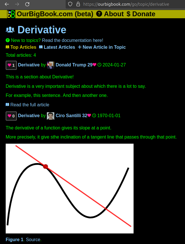
Figure 1. Screenshot of the "Derivative" topic page. View it live at: ourbigbook.com/go/topic/derivativeVideo 2. OurBigBook Web topics demo. Source. - local editing: you can store all your personal knowledge base content locally in a plaintext markup format that can be edited locally and published either:This way you can be sure that even if OurBigBook.com were to go down one day (which we have no plans to do as it is quite cheap to host!), your content will still be perfectly readable as a static site.
- to OurBigBook.com to get awesome multi-user features like topics and likes
- as HTML files to a static website, which you can host yourself for free on many external providers like GitHub Pages, and remain in full control

Figure 2. You can publish local OurBigBook lightweight markup files to either OurBigBook.com or as a static website.
Figure 3. Visual Studio Code extension installation.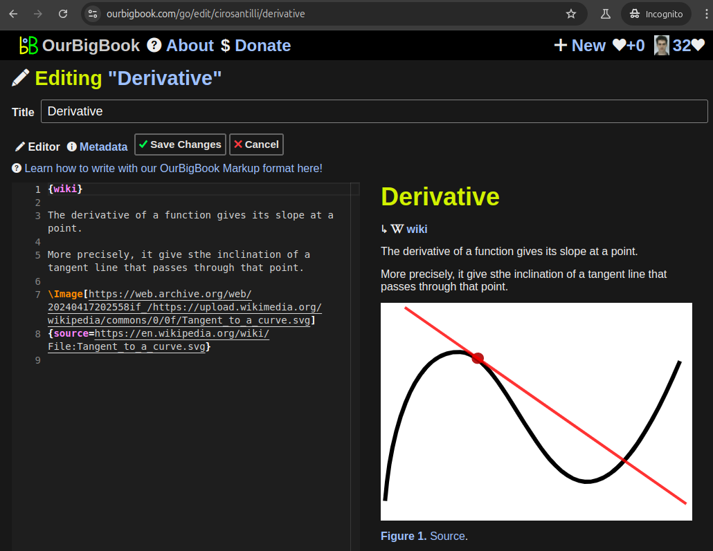
Figure 5. . You can also edit articles on the Web editor without installing anything locally. Video 3. Edit locally and publish demo. Source. This shows editing OurBigBook Markup and publishing it using the Visual Studio Code extension. 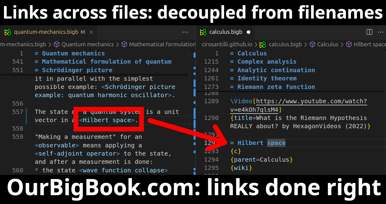
- Infinitely deep tables of contents:
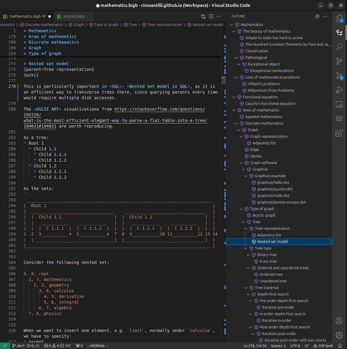



All our software is open source and hosted at: github.com/ourbigbook/ourbigbook
Further documentation can be found at: docs.ourbigbook.com
Feel free to reach our to us for any help or suggestions: docs.ourbigbook.com/#contact