
Each concentric shell has a different circumference, so it generally needs a different integer wrapping vector . Different vector lengths do not force different chiral angles, but exact atomic registry between all curved shells is geometrically restrictive. The shells can nucleate with different wrapping orientations, and strong covalent bonding within each shell dominates the weaker intershell interaction.
Consequently, it is usually unnecessary to strain every shell into a common orientation and registry; many multiwall tubes have incommensurate shells with different chiral angles. Identical chiral angles are possible, for example among suitable members of one armchair family, and should not be ruled out purely because the radii differ. Atomic indices, chiral angle and interwall commensurability are distinct descriptions.
The circumference is the length of the graphene wrapping vector:For ,Approximating the closest wall-to-wall separation by the graphite interlayer spacing gives the nearest-neighbour axis separation in a triangularly packed bundle:This assumes undeformed circular tubes with a graphitic contact gap. Faceting, flattening, adsorbates or pressure can alter a real bundle's spacing.
In floating-catalyst CNT growth, a controlled sulfur additive acts as a growth promoter for the catalyst, commonly iron. Sulfur modifies catalyst surface composition, carbon uptake and the strength of the catalyst-carbon interaction; it can facilitate cap formation/lift-off and sustained tube growth instead of complete catalyst encapsulation. It also changes catalyst-particle evolution and hence tube yield, diameter and wall-count distributions.
There is an optimum range: excessive sulfur can occupy active sites or form an insufficiently active sulfide-rich catalyst and reduce growth. The additive is not simply a constituent that must be incorporated into every carbon wall. Its detailed action depends on catalyst, carbon source and process conditions; a single universal melting-point explanation is insufficient.[ref]
The promoter role of sulfur in carbon nanotube growth by Balázs Orbán and Tibor Höltzl. First-principles evidence for sulfur weakening iron-carbon binding; later mechanistic support, not an official answer
Relative to conventional crystalline-silicon technology, many organic absorbers offer low-temperature thin-film processing and lightweight flexible devices, but have more strongly bound excitons and more disorder-limited charge transport. These are common material trends, not universal statements about every organic or inorganic device.
Relevant semiconductor properties include the absorption spectrum and optical gap, donor/acceptor energy levels and offsets, dielectric screening and exciton dissociation, electron/hole mobilities, recombination lifetimes, traps and morphological stability. Contacts must extract the appropriate carrier selectively. These properties determine the device quantities inA favourable gap alone does not fix efficiency: current generation, voltage loss and fill factor must all be controlled.
A suitable donor-acceptor heterojunction provides an energetically favourable route from a bound excitation to an interfacial charge-transfer state and then separated carriers. The electron is preferentially transported in the acceptor and the hole in the donor. The interface facilitates dissociation that is inefficient in a single strongly excitonic material; it must also avoid excessive energy loss and rapid interfacial recombination.
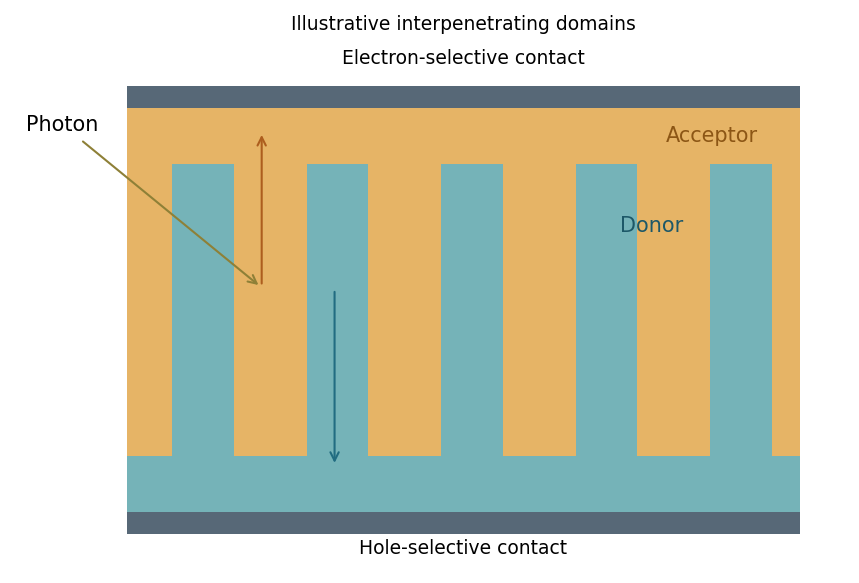
An interpenetrating donor-acceptor structure balances short exciton travel with continuous charge-extraction paths
. Source. Details. An idealized bulk heterojunction places most generated excitons within roughly a diffusion length of an interface while maintaining continuous donor paths to the hole contact and acceptor paths to the electron contact. Domain dimensions should therefore be comparable to the material's exciton transport scale, not arbitrarily large. The total absorbing thickness should capture substantial light yet remain within the charge-collection capability set by mobility, field and recombination. Excessive mixing can impair transport or increase recombination; very coarse domains waste excitons before they reach an interface.[ref]
An exciton is a Coulomb-correlated electron-hole pair, electrically neutral overall. Three useful properties are:
- Exciton binding energy: the energy required to separate the correlated pair into unbound carriers. A larger value makes thermal dissociation less effective; dielectric screening and electronic delocalization influence it.
- Spatial extent: the characteristic electron-hole separation or exciton radius. A localized Frenkel-like exciton is small compared with a Wannier-Mott exciton spread over many unit cells.
- Lifetime: the characteristic time before radiative or nonradiative decay. Together with its diffusion coefficient it determines a transport scale, often expressed as in a specified diffusion-length convention.
In many molecular organic semiconductors, limited screening and localization make exciton binding important, so absorption need not immediately produce collectable free charges.
Two examples are poly(3-hexylthiophene), P3HT, a conjugated polymer commonly used as an electron donor, and PCBM, a soluble fullerene derivative commonly used as an electron acceptor. Both are organic semiconductors; “organic” does not imply that their transport properties are identical. Their blend is a familiar donor-acceptor photovoltaic model system.
In a vibrating-sample magnetometer, a magnetized specimen vibrates sinusoidally in a nominally uniform applied field. Its motion changes the magnetic flux through stationary pickup coils, producing an induced voltage by Faraday's law of induction. The component at the vibration frequency is proportional to the sample magnetic moment times vibration amplitude and frequency, for a calibrated coil geometry.
A lock-in detector referenced to the vibration extracts this small signal. Calibrate with a known moment, stabilize the vibration amplitude and sweep the applied field to measure a magnetization loop. Dividing moment by film volume gives in ; the silicon substrate and holder background must be subtracted for such a thin film.[ref]
For a clean, adiabatically connected GaAs channel at low temperature and small bias, opening successive spin-degenerate subbands givesConductance therefore shows a staircase of plateaux, rather than the continuously geometry-dependent classical Ohmic result. Each fully transmitted mode contributes approximately . More positive, or less negative, depletion-gate voltage opens a conventional GaAs constriction; more negative voltage closes it.
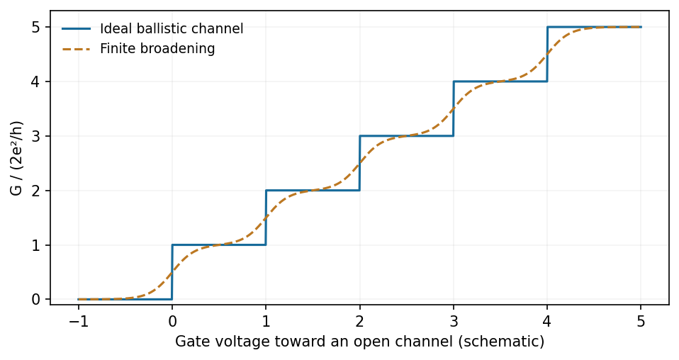
Require subband spacings larger than thermal and bias broadening and a mean free path exceeding the constriction length. The general Landauer formula is with each spin/valley channel counted separately. A material with additional valley degeneracy need not have the same step sequence as GaAs, and imperfect transmission or contact resistance blurs the ideal plateaux.
One suitable platform is a monolayer molybdenum disulfide semiconductor. An electrostatic accumulation gate supplies conduction electrons whose motion is confined to the atomic sheet; source and drain contacts act as reservoirs. A clean insulating substrate and dielectric or encapsulation reduce disorder and prevent gate leakage. Two split gates deplete the adjacent sheet and leave a narrow conducting gap, thereby confining the in-plane transverse direction while retaining transport along the gap.
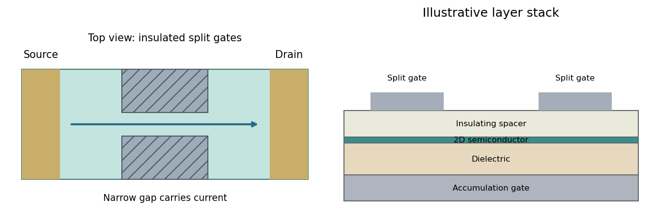
Apply a small source-drain voltage, measure the current and determine linear-response conductance while tuning the split-gate voltage and carrier density. A graphene sheet is another two-dimensional carrier system, but its lack of an ordinary gap complicates purely electrostatic confinement; etched boundaries or a suitable gapped architecture may be needed. A two-dimensional material does not by itself guarantee ballistic transport or resolved subbands.[ref]
Split-gated point-contact in MoS2-hBN structures by Chithra H. Sharma and Madhu Thalakulam. Electrostatic confinement in a two-dimensional semiconductor platform
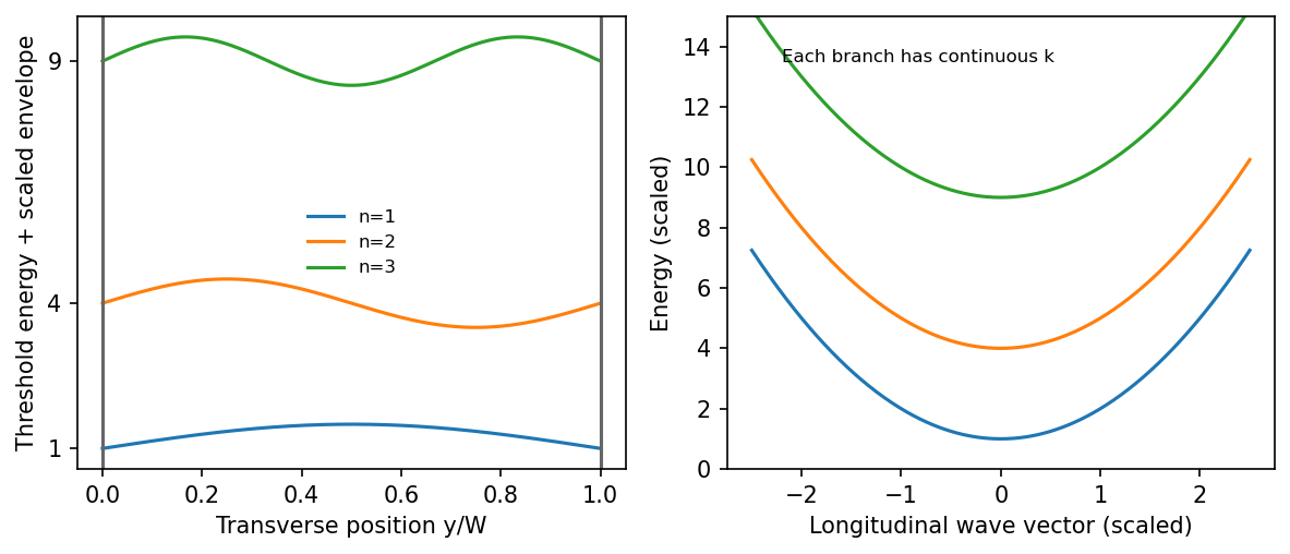
Let run along the wire and across it. In a separable approximation,Transverse confinement gives discrete levels , but the long unconfined direction has a nearly continuous longitudinal wave vector and a plane-wave factor. The result is a family of one-dimensional subbands, not a completely discrete spectrum in both in-plane directions. For a hard-wall width , ; an electrostatic confinement potential gives different thresholds. The suppressed out-of-plane degree of freedom is already frozen into the 2DEG subband.


Use complementary composition, spatial and population measurements:
- Insufficient Pt: digest representative aliquots and measure calibrated ICP-OES or ICP-MS to obtain bulk Pt/Pd ratio and trace Fe. Blanks, recovery checks and standards control contamination and matrix effects. This is sensitive and quantitative but destructive and supplies no particle-by-particle spatial information.
- Poor Pt-Pd mixing: use STEM-EDS maps or line profiles of many individual particles. Characteristic X-ray energies identify the elements; background subtraction and calibrated sensitivity factors permit local composition estimates. HAADF-STEM supplies complementary atomic-number-sensitive contrast, with Pt generally brighter than Pd for comparable thickness. Core-shell segregation or distinct domains can then be tested. Projected overlap can imitate mixing, and low counts, thickness and beam damage limit nanoscale quantification; tomography or multiple views can resolve important ambiguities.
- Fe impurities: EDS/EELS can locate Fe-rich inclusions or surface-associated material, while the bulk digest establishes whether a trace signal is representative. Failure to detect Fe in a few TEM fields does not rule out dilute contamination below local detection limits. XPS can additionally assess near-surface composition and oxidation state, but is not a bulk assay.
- Size uniformity: obtain calibrated TEM images from randomly chosen independent fields, segment individual particles and report a number-weighted size histogram with sample count and shape descriptors. Avoid overlap and selection of only well-dispersed or attractive particles. A projected diameter is not a complete three-dimensional volume; scattering methods can corroborate ensemble size but weight particles differently.
A bulk fcc atom has twelve nearest neighbours, whereas surface atoms are undercoordinated: ideal (111) terrace atoms have nine and (100) terrace atoms eight. Steps, kinks, edges and corners can have still lower coordination and different bond-angle environments. These sites change electronic structure, adsorption energies and activation barriers, making geometrically different sites catalytically inequivalent.
In a Pt-Pd particle, a site's neighbours may be Pt, Pd or a mixture; surface segregation means surface composition need not equal overall composition. Alloying also changes strain and electronic interactions. Surface relaxation, reconstruction, adsorbed ligands, oxide or contamination can further alter accessibility and chemical state. A high nominal Pt fraction therefore does not establish either accessible Pt sites or a particular catalytic activity.
In cluster-beam deposition, evaporated or sputtered cobalt atoms cool in an aggregation gas, nucleate clusters and are carried to a substrate. Source temperature, gas pressure, aggregation length and residence time tune the mean size and distribution. A mass selector can narrow the delivered size range, at the cost of transmitted flux; an unfiltered beam does not automatically produce monodisperse particles.
Shape control is less direct. Growth kinetics and cluster temperature can favour particular structures, while multiple morphologies can coexist at one size. Landing energy, substrate interactions and post-deposition annealing can change the delivered shape or cause coalescence. Soft landing helps preserve gas-phase clusters. In solution, ligands, selective facet binding, seed-mediated growth and precursor feeding can give stronger chemical control over shape and size, but introduce ligand/solvent residues and require purification. Neither method guarantees a unique shape merely by selecting particle size.
The Winterbottom construction extends the Wulff construction to a crystal supported on a substrate. It includes the particle-substrate interfacial energy and the substrate surface energy displaced by contact, so the equilibrium Wulff body is truncated by the support plane. The relevant contact contribution is ; it determines wetting and contact geometry. The basic unsupported construction accounts only for orientation-dependent free surface energies.[ref]
Equilibrium shape of a small particle in contact with a foreign substrate by W. L. Winterbottom. Supported-particle equilibrium construction
There are unlisted articles, also show them or only show them.