A semiconductor has a filled valence band and an empty conduction band at zero temperature in the intrinsic idealisation, separated by a modest band gap. Thermal excitation or deliberately introduced impurities can create mobile Electrons and electron holes. Its conductivity is consequently very sensitive to temperature and doping. A metal has available electronic states at the occupied energy boundary, through a partly filled band or overlapping bands, and need not thermally excite carriers across a gap.
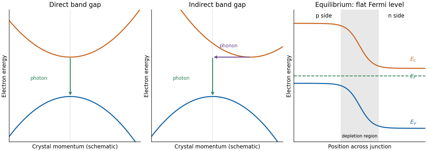
For a direct band gap, the conduction-band minimum and valence-band maximum occur at the same crystal momentum. An Electron can recombine with a hole near these extrema and emit a photon while conserving crystal momentum, since optical photon momentum is small on the lattice scale. For an indirect band gap, the extrema lie at different crystal momenta. A band-edge radiative transition then ordinarily needs a phonon as well, making it less probable and allowing nonradiative processes to compete more effectively.
gallium arsenide has a direct fundamental gap, while silicon has an indirect one. This makes efficient band-edge emission and hence a light-emitting diode easier to obtain from gallium arsenide. It does not mean silicon has no optical transitions or that every direct-gap sample emits efficiently: defects, surfaces and carrier confinement also matter.
Semiconductor doping introduces impurities with levels close to the band edges. A donor impurity can release an Electron to the conduction band, leaving a fixed positive ion; an n-type semiconductor has Electrons as majority carriers. An acceptor impurity can take an Electron from the valence band, leaving a mobile hole and fixed negative ion; a p-type semiconductor has holes as majority carriers. The opposite species remains as a minority carrier population, and a neutral bulk sample balances the ionised dopants with mobile carriers.
At a p-n junction, concentration gradients initially drive Electrons and holes across the join. Their removal near the join exposes negative acceptor ions on the p side and positive donor ions on the n side, forming a depletion region. Its electric field opposes further majority-carrier diffusion. Equilibrium has a flat Fermi level, no net current and spatially bent band edges. With p on the left and n on the right, the Electron band edges fall towards the n side; the difference is the equilibrium barrier in Electron energy. A flat Fermi level does not mean flat conduction and valence edges.

For a hydrogenic donor state, replace the bare Electron mass by and the Coulomb permittivity by with . Rescaling the Bohr model gives the positive ground-state binding magnitudeThe radius isusing the Bohr radius . The supplied positive hydrogen “energy” formula should be interpreted as a binding magnitude; the bound level's energy relative to the conduction-band edge is .
At , , about five times the binding energy. Thus a substantial fraction, ordinarily most of the shallow donors in the dilute nondegenerate regime, will be ionised. An exact fraction also depends on the Fermi level, donor concentration and degeneracies; comparing with alone does not determine it exactly. The large radius explains why a weakly bound donor extends across many unit cells.
The atomic number density isOne fully ionised single-electron donor per million atoms givesThe usual simplified answer treats conductivity as proportional to Electron concentration and assumes unchanged electron mobility, giving about times the undoped conductivity. There is a qualification: the conductivity ratio of doped and intrinsic semiconductors is not fixed by Electron counts alone. Intrinsic material also has , whereas the heavily n-type sample has and . ThereforeWith unchanged Electron mobility and negligible intrinsic hole conductivity this reduces to ; with equal, unchanged Electron and hole mobilities it is about . The problem supplies no mobilities, so the density-ratio estimate requires its stated approximation. Ionised impurities may additionally reduce mobility.
Use a Hall effect measurement. Pass a known current through a thin rectangular specimen, apply a perpendicular magnetic field , and measure the transverse Hall voltage . For a uniform single-carrier sample of thickness ,The Hall-voltage sign identifies the carrier sign. Reverse and the current to separate the field-odd Hall signal from voltage-probe misalignment and offsets, and measure the specimen thickness accurately. The extraction assumes a one-carrier Hall factor near one. In intrinsic or mixed-carrier material, the two-carrier Hall coefficient is mobility weighted, so Hall voltage and conductivity need a two-carrier interpretation rather than this simple inverse formula.
For donor number density , the mean separation is of order . A donor-state overlap estimate sets this scale comparable with the effective radius:Relative to the atomic density, this is , about parts per million. If “start to overlap” is defined geometrically by centre separation , the estimate is instead , about parts per million. Thus the geometric estimate is of order –. Real donor wavefunctions have tails, not hard orbit edges, so this does not define a sharp threshold or by itself locate a metal-insulator transition.
Articles by others on the same topic
There are currently no matching articles.