A phonon is one quantum of a crystal's vibrational normal modes. In the harmonic approximation, each mode is a quantum harmonic oscillator with energy levels . A phonon carries excitation energy and crystal momentum modulo a reciprocal lattice vector. It is a collective lattice excitation, not one atom travelling along the chain. Phonons obey Bose-Einstein statistics; their number need not be conserved in thermal equilibrium.
Put type-A atoms at and type-B atoms at . Their displacements obey Newton's second law,Choose normal modes and . Substitution givesA nonzero displacement vector requires zero determinant:Solving this quadratic in gives the diatomic-chain dispersion relation with equal springs,The primitive unit cell has length , so the first Brillouin zone is .
The minus solution is the acoustic phonon branch. As , tends to zero and : adjacent atoms move together in a long-wavelength compression. The plus solution is the optical phonon branch, with nonzero zone-centre frequency and : the two sublattices move against one another with fixed cell centre of mass. For oppositely charged ions, this relative displacement can couple to an electric field, motivating the optical name.
At the zone boundary the frequencies are and . Different masses produce a gap; equal masses make the two branches meet, recovering a folded monatomic dispersion.
Put and use . Expanding the square root givesThus, to leading nonzero orders,The absolute value ensures a nonnegative angular frequency for either direction. The speed of sound is the initial acoustic slope .
The vertical axis of the original figure is angular frequency, in , not ordinary frequency. Its zone-centre optical intercept is approximately . Convert the relative atomic masses using :The long-wavelength inference of diatomic-chain parameters then givesNo factor is needed because the graph already plots .
Reading near the origin, an acoustic point is approximately . The initial slope therefore estimatesCombining the slope with the inferred spring constant givesThis is the model's adjacent Na-plane to Cl-plane spacing; its cell length is . The slope is a graphical estimate, so values around – and spacings near are consistent with the reading precision. A real ionic crystal has interactions beyond the scalar nearest-neighbour model; an intercept-and-slope fit need not reproduce the entire measured dispersion or independently measured structural spacing exactly.
A semiconductor has a filled valence band and an empty conduction band at zero temperature in the intrinsic idealisation, separated by a modest band gap. Thermal excitation or deliberately introduced impurities can create mobile Electrons and electron holes. Its conductivity is consequently very sensitive to temperature and doping. A metal has available electronic states at the occupied energy boundary, through a partly filled band or overlapping bands, and need not thermally excite carriers across a gap.
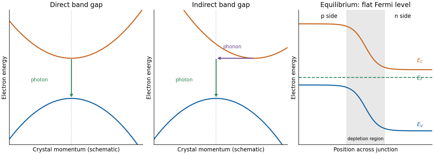
For a direct band gap, the conduction-band minimum and valence-band maximum occur at the same crystal momentum. An Electron can recombine with a hole near these extrema and emit a photon while conserving crystal momentum, since optical photon momentum is small on the lattice scale. For an indirect band gap, the extrema lie at different crystal momenta. A band-edge radiative transition then ordinarily needs a phonon as well, making it less probable and allowing nonradiative processes to compete more effectively.
gallium arsenide has a direct fundamental gap, while silicon has an indirect one. This makes efficient band-edge emission and hence a light-emitting diode easier to obtain from gallium arsenide. It does not mean silicon has no optical transitions or that every direct-gap sample emits efficiently: defects, surfaces and carrier confinement also matter.
Semiconductor doping introduces impurities with levels close to the band edges. A donor impurity can release an Electron to the conduction band, leaving a fixed positive ion; an n-type semiconductor has Electrons as majority carriers. An acceptor impurity can take an Electron from the valence band, leaving a mobile hole and fixed negative ion; a p-type semiconductor has holes as majority carriers. The opposite species remains as a minority carrier population, and a neutral bulk sample balances the ionised dopants with mobile carriers.
At a p-n junction, concentration gradients initially drive Electrons and holes across the join. Their removal near the join exposes negative acceptor ions on the p side and positive donor ions on the n side, forming a depletion region. Its electric field opposes further majority-carrier diffusion. Equilibrium has a flat Fermi level, no net current and spatially bent band edges. With p on the left and n on the right, the Electron band edges fall towards the n side; the difference is the equilibrium barrier in Electron energy. A flat Fermi level does not mean flat conduction and valence edges.

For a hydrogenic donor state, replace the bare Electron mass by and the Coulomb permittivity by with . Rescaling the Bohr model gives the positive ground-state binding magnitudeThe radius isusing the Bohr radius . The supplied positive hydrogen “energy” formula should be interpreted as a binding magnitude; the bound level's energy relative to the conduction-band edge is .
At , , about five times the binding energy. Thus a substantial fraction, ordinarily most of the shallow donors in the dilute nondegenerate regime, will be ionised. An exact fraction also depends on the Fermi level, donor concentration and degeneracies; comparing with alone does not determine it exactly. The large radius explains why a weakly bound donor extends across many unit cells.
The atomic number density isOne fully ionised single-electron donor per million atoms givesThe usual simplified answer treats conductivity as proportional to Electron concentration and assumes unchanged electron mobility, giving about times the undoped conductivity. There is a qualification: the conductivity ratio of doped and intrinsic semiconductors is not fixed by Electron counts alone. Intrinsic material also has , whereas the heavily n-type sample has and . ThereforeWith unchanged Electron mobility and negligible intrinsic hole conductivity this reduces to ; with equal, unchanged Electron and hole mobilities it is about . The problem supplies no mobilities, so the density-ratio estimate requires its stated approximation. Ionised impurities may additionally reduce mobility.
Use a Hall effect measurement. Pass a known current through a thin rectangular specimen, apply a perpendicular magnetic field , and measure the transverse Hall voltage . For a uniform single-carrier sample of thickness ,The Hall-voltage sign identifies the carrier sign. Reverse and the current to separate the field-odd Hall signal from voltage-probe misalignment and offsets, and measure the specimen thickness accurately. The extraction assumes a one-carrier Hall factor near one. In intrinsic or mixed-carrier material, the two-carrier Hall coefficient is mobility weighted, so Hall voltage and conductivity need a two-carrier interpretation rather than this simple inverse formula.
For donor number density , the mean separation is of order . A donor-state overlap estimate sets this scale comparable with the effective radius:Relative to the atomic density, this is , about parts per million. If “start to overlap” is defined geometrically by centre separation , the estimate is instead , about parts per million. Thus the geometric estimate is of order –. Real donor wavefunctions have tails, not hard orbit edges, so this does not define a sharp threshold or by itself locate a metal-insulator transition.
Articles by others on the same topic
There are currently no matching articles.