An electronic amplifier uses an electrical power supply to increase a signal's amplitude or available output power. The input controls the transfer of supply energy to the load; it does not supply all the amplified output energy itself.
A voltage amplifier, a transimpedance amplifier and a charge amplifier relate different input and output quantities. To characterize one, vary the input around its operating point and measure gain, frequency response, noise and the range before saturation. A large gain does not by itself improve signal-to-noise ratio, since input noise and amplifier noise can both be amplified.
Electronic gain expresses how an electronic circuit scales a specified input signal quantity into an output quantity. For a linearized voltage amplifier around its operating point, the voltage gain is . At a sinusoidal frequency it can be a complex phasor ratio, specifying both amplitude ratio and phase shift. Power gain instead compares the average power delivered to the load with the average signal power entering the amplifier:State the input/output quantities, frequency, load and operating conditions when specifying gain. A transimpedance amplifier relates output electric potential difference to input current and has a dimensional transfer ratio in ohms.
For an original circuit example, use an inverting operational amplifier with input resistor , feedback resistor and load . In its ideal negative-feedback linear regime,An input of root mean square therefore gives root mean square at the output, with a phase inversion. The manufacturer's primary explanation derives this resistance-ratio gain using the input and feedback currents.[ref]
Op-Amps, Comparator Circuit by Renesas. Op-Amp Basics (1), Figure 2 and the derivation of the inverting gain
Suitable supplies, output-current capability and amplifier output range are assumptions of this worked model, not specifications of a particular device.Here the input resistance is in the ideal model. For resistive ports and root-mean-square signal amplitudes,The example input power is and load power , giving . The additional output energy comes from the amplifier's supply, controlled by the input signal. The impedance condition for converting voltage gain to power gain is essential: voltage magnitude alone does not specify load power.
Voltage gain is conventionally expressed as decibels, while power gain uses . This example has voltage gain and power gain ; the two expressions agree when the resistive input and load impedances are equal. A negative voltage gain indicates phase inversion; its magnitude enters the logarithm.
A direct test drives a small sine wave into the input and measures the actual terminal signals with an oscilloscope. Sweeping frequency reveals the frequency response; increasing amplitude reveals amplifier clipping or other departure from the assumed linear gain. Keep the load and measurement impedances specified. Gain can amplify input noise along with signal, so the signal-to-noise ratio requires its own measurement.
A voltage gain determines a power gain only when the electrical conditions at both ports are included. The familiar equality between and requires a particular impedance relation; it is not a conversion between arbitrary voltage and power ratios.
Use phasors whose moduli are root mean square amplitudes, at one sinusoidal frequency. At a load with electrical impedance and electrical admittance , the current is . Its complex electrical power is , with the complex conjugate arising from the relative phase of the two sinusoids. Averaging over a cycle gives the active powerTo see the averaging step, write and similarly for . The product's cycle average is , the real part of . Peak-amplitude phasors instead require an extra factor .
Let describe the actual input impedance and the actual load impedance. Take and with nonzero terminal signals, and define currents into the amplifier at the input and into the load at the output. With the measured loaded voltage gain ,Thus requires equality of the relevant electrical conductances, not merely equality of impedance moduli. For example, input and load both have modulus , but their electrical admittances have real parts and . The multiplier is , so .
For real resistive ports this becomesTake an original example with measured , and . The voltage gain is , while the power gain is , or . An active buffer can reduce the signal's electric potential difference while delivering more signal power than it accepts at its input; the supply provides the additional energy.
The amplifier's output impedance is distinct from the connected load impedance. To show why that distinction matters, model its output by a Thévenin equivalent with open-circuit voltage and series resistance . The voltage divider givesWith and , the load produces the preceding example. Differentiating gives , so delivered power is largest at , as in the maximum power transfer theorem. Here its power gain is . Increasing much further makes approach but reduces delivered power. That high-load-impedance regime is impedance bridging, useful for sensing the source's voltage with little loading.
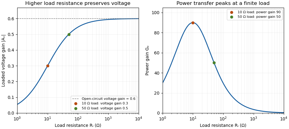
A bench demonstration uses a function generator, a known termination and an oscilloscope. The Keysight guide explains that an expected-load setting changes how amplitude is displayed for generators with a fixed series output impedance; a high-impedance load can receive twice the voltage expected for a matched termination.[ref]
Output Load Termination in the Keysight BenchVue Function Generator documentation. Output Load Termination, fixed output impedance and the 50-ohm/open-circuit examples
As an independent low-frequency resistive calculation, an open-circuit source of root mean square with series resistance delivers and to . Into it delivers about but only . The larger terminal reading accompanies much less delivered power. Specify the actual load, frequency and amplitude convention when comparing gain measurements.An instrumentation amplifier amplifies a differential input while presenting high input impedance and rejecting a common component. A useful ideal relation isIts common-mode rejection ratio describes finite unwanted response to common-mode voltage. This is distinct from the amplifier input common-mode range over which the circuit can operate without internal saturation.[ref]
A Practical Review of Common Mode and Instrumentation Amplifiers by Eamon Nash. Introduction; equations1–2 and Common Mode Voltage Range
For an original example, stipulate , , and . The differential signal is and the ideal output is , assuming all input and output limits are satisfied.
Now suppose the differential-to-common gain ratio is , or . The common-mode gain is then . A common-input change contributes at the output, five percent of the desired signal contribution. A high rejection ratio therefore does not mean zero error.
A source that changes both inputs together tests rejection; a source that changes their difference tests differential gain. Both tests must respect input common-mode limits, amplifier output range, load and frequency response. A plausible ideal output value alone does not prove that every internal stage remains linear.
The amplifier input common-mode range is the set of common-mode voltages for which an electronic amplifier meets its operating requirements at the specified differential input, gain, supplies and load. A high common-mode rejection ratio describes rejection within a usable operating region; it does not extend that region. An instrumentation amplifier can have saturated internal stages even when its ideal final output fits the amplifier output range.[ref]
A Practical Review of Common Mode and Instrumentation Amplifiers by Eamon Nash. Three Op-Amp Instrumentation Amplifier, Common Mode Range, Figure5
An original simplified three-amplifier model makes the constraint visible. Let the input-stage output potentials bewhere and . Suppose each internal output must stay between and . ThenFor and , the permitted common interval is –. Choosing predicts internal outputs and and violates the stipulated limit. A unity-gain difference stage with reference would nevertheless predict a plausible final . That final prediction alone is insufficient.
This is an illustrative architecture model, not a device specification; input-device limits can impose further restrictions. A practical test holds fixed while sweeping both inputs together, recording differential gain error and distortion. Repeat at the intended gain and differential amplitudes. The resulting operating region is more informative than a single common-mode interval quoted without its test conditions.
The amplifier output range is the interval over which an electronic amplifier can provide the specified output behavior under stated supply, load and operating conditions. Its limits need not coincide with the power-supply potentials. The historical integrator datasheet lists output range and output-current conditions separately from its supply conditions.[ref]
ACF2101 Low Noise, Dual Switched Integrator datasheet. Electrical Specifications, pp2–3, test conditions and Output section
For an original linear model, let with positive gain. Avoiding static clipping requiresStipulate a – supply, usable output limits –, and . The permitted differential input interval is to . A positive input predicts and fits; a negative input predicts and does not.
These are stipulated limits, not a product guarantee. The amplifier output headroom relative to each supply can differ. Loading can change the available output swing, and input-stage saturation can occur even when the final ideal output lies inside its range. A slow input sweep identifies the static departure from linear gain; a pulse test additionally probes dynamic recovery. Amplifier clipping describes the waveform consequence of exceeding these limits.
Amplifier output headroom is the electric potential difference reserved between a usable output limit and its corresponding supply rail. If the supply potentials are and the specified amplifier output range is , defineThese two margins can differ and depend on load and operating conditions. The switched-integrator datasheet lists supply conditions, output range and output-current limits separately.[ref]
ACF2101 Low Noise, Dual Switched Integrator datasheet. Electrical Specifications, pp2–3, Output and Power Supply
For an original chosen – circuit with usable limits and , the lower and upper margins are and . A signal centered at has maximum symmetric peak excursionAt this is . Centering instead at permits . Thus centering on the supply midpoint need not maximize the usable symmetric swing.
An output sweep into the actual load identifies where the specified gain or distortion tolerance fails. Changing the load tests whether the limit comes from output-current demand. These measurements concern static headroom; a fast pulse also tests frequency response and overload recovery. More final-stage headroom does not cure an internal violation of the amplifier input common-mode range.
Amplifier clipping occurs when an electronic amplifier cannot follow the output amplitude predicted by its small-signal voltage gain. Its finite amplifier output range truncates the waveform. For a deliberately simple, instantaneous model with positive gain and fixed lower and upper output limits,Here and are input and output electric potential differences. The flat portions express a nonlinearity: doubling an already excessive input need not change the output. Real output limits depend on the supply, load and output stage. They need not equal the supply rails. Texas Instruments' example integrating amplifier uses separate supply and output-range design goals and explains how unrestricted DC integration eventually reaches saturation.[ref]
Integrator Circuit by Pete Semig. p1, Design Goals and Design Description
Amplifier clipping can corrupt an area measurement even when the waveform still looks easy to integrate. Suppose , , , and a rectangular input is for and zero otherwise. Its true area is , but the ideal unclipped output of is reduced to . Dividing the clipped waveform area by the gain gives50% below the true input area. Any rectangular input at or above with the same duration produces this same clipped plateau in the stipulated model. Subsequent integration cannot recover which of those input amplitudes was present.
A useful bench experiment feeds a repeatable pulse into an electronic amplifier and records both input and output on an oscilloscope. Increase the input amplitude while holding the gain, pulse duration and load fixed. The output first scales with the input, then ceases to do so near its limits. Reducing the gain tests whether an apparent input plateau is actually a receiver limit. Comparing measured areas before and after that change reveals the clipped waveform area bias directly.
The instantaneous clipping formula does not describe the internal dynamics of a saturated integrating amplifier. Once its feedback assumptions fail, recovery can take additional time. The ACF2101's historical datasheet explicitly distinguishes output overload from ordinary reset and describes extra recovery delay; the relevant behavior must be characterized for the actual circuit.[ref]
ACF2101 Low Noise, Dual Switched Integrator datasheet. p10, Output Overload
An integrator reset establishes a new starting state, while a suitable input range prevents information being lost before that reset.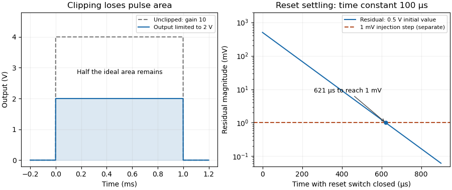
Ideal pulse clipping loses area, while a finite reset leaves an exponentially decreasing residual; the separate dashed level illustrates a stipulated charge-injection pedestal.
Details. A clipped waveform area is the integral of an amplitude-limited trace over the specified interval. It can differ from the unclipped area by a different proportion than the change in peak height. The amplifier clipping article gives the instantaneous limiter model and a rectangular-pulse example; real saturated integrators can also have recovery dynamics.[ref]
ACF2101 Low Noise, Dual Switched Integrator datasheet. p10, Output Overload
An original triangular example takes with . Its true area is . Clip its top at , with the zero baseline unchanged. The missing region is a triangle of height and base , soFor , and , the area falls from to . The peak is halved but the area loses only . The clipping loss for a triangular pulse therefore cannot be inferred merely by applying the peak-loss percentage to its integral.
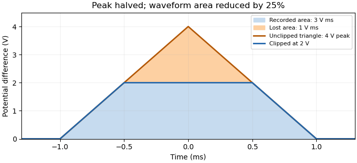


Record input and output together while changing gain or attenuation to test whether the trace is clipped. Recovering area by fitting an assumed triangle is a model-based correction, not recovery of an arbitrary waveform from its plateau. Baseline errors, limited bandwidth and overload recovery require their own measurement models.
The clipping loss for a triangular pulse is the area removed when a triangular waveform exceeds an amplitude limit. In the ideal model of clipped waveform area, and the upper limit is . The original area is ; the missing top triangle has areaThe geometry is derived in clipped waveform area, with its original diagram. Here is the half-width of the full support, not the width of the clipped plateau.
A useful inverse problem asks how much peak truncation an area-error tolerance permits. If the allowable fractional loss is , the ideal triangle requiresFor an original , pulse, a area-loss allowance requires . At equality, the peak is reduced by but the area changes from to . The plateau duration is only . This is a shape-dependent calculation, not a universal relationship between peak error and integral error.
An attenuated simultaneous trace can test whether the input is approximately triangular and whether its duration stays fixed as amplitude changes. Baseline and bandwidth must be comparable before an area ratio is meaningful. A real saturated integrating amplifier can have additional overload recovery, which the instantaneous clipping model omits.[ref]
ACF2101 Low Noise, Dual Switched Integrator datasheet. p10, Output Overload
The formula supplies a conditional error estimate; it cannot identify an arbitrary missing waveform from its plateau.An integrating amplifier produces an output proportional to the time integral of its input over an intended operating range. A common circuit uses an operational amplifier, an input resistor and a feedback capacitor . With the non-inverting input held at zero, ideal negative feedback maintains a virtual ground at the inverting input. Negligible amplifier input current then givesThe initial output records the capacitor's initial charge. Texas Instruments' circuit note derives this inverting relation and explains why real integration is limited by the circuit time constant and amplifier bandwidth.[ref]
For an original example, choose and , so . A constant0.20volt input lasting2milliseconds changes the output by . Repeating ten such pulses without intervening input or integrator reset changes it by in the ideal model. The output retains information about accumulated pulse area, rather than only the present input value.
A small offset also accumulates. With the same components, a residual input-equivalent1millivolt gives a slope of . Starting from zero, an idealized negative output limit at5volts would be reached in5seconds. The finite supply range causes amplifier clipping; an ideal integral extending indefinitely is not physically available.
Putting a resistor in parallel with the feedback capacitor supplies a DC path. Under ideal amplifier assumptions its zero-state transfer function isAt frequencies where , this approaches ; at low frequency it instead approaches the finite gain . The resistor prevents unrestricted DC accumulation while changing the lowest usable integration frequency.[ref]
An integrating amplifier can therefore turn a short detector pulse into a measurable accumulated output, but its initial condition, reset, baseline, frequency range and output limits belong to the measurement model. A charge amplifier is a related current-input arrangement in which collected charge is converted through feedback capacitance.
An integrator reset establishes the charge on an integrating amplifier's feedback capacitor before the next measurement. Without it, the next output includes the previous initial condition, and repeated input pulses or input offset voltage can eventually cause amplifier clipping. Resetting makes consecutive measurement intervals comparable; it does not reconstruct a pulse already lost to amplifier clipping.
Consider an inverting integrating amplifier with the input held at zero during reset. Place an analog switch across its feedback capacitor . In the approximation of a stable ideal operational amplifier maintaining a virtual ground, a closed switch with constant on-state electrical resistance gives the RC circuit relationThis exponential decay gives an integrator reset settling time for residual magnitude at most :For stipulated values , and , the reset time constant is . Reaching a residual of requires about in this model. Actual amplifier drive, stability and recovery from overload can change the response. A switch's control delay also differs from the full circuit's settling time.[ref]
MT-088: Analog Switches and Multiplexers Basics. pp11–13, Figures19–21: settling versus switching delay
Opening the reset switch can itself disturb the initial condition. Analog switch charge injection transfers a small charge to the connected capacitor, producing a reset charge-injection pedestal of magnitudeFor a stipulated deposited on , this step is . Its sign depends on the circuit and charge direction. A longer reset suppresses the preceding exponential residual but need not suppress the new step created when the switch opens. Analog Devices illustrates this capacitive coupling mechanism and the resulting output step separately from retained-charge settling.[ref]
MT-088: Analog Switches and Multiplexers Basics. pp9–10, Figures13–16
A practical experiment repeats zero-input measurements with several reset durations and reads the output at the same delay after switch opening. A decreasing residual indicates incomplete discharge; a persistent offset can instead include reset charge-injection pedestal, input offset voltage and subsequent drift. Repeated readings help separate the reproducible offset from noise. The ACF2101 provides a concrete historical implementation: separate hold and reset controls disconnect the input and discharge the integration capacitor, and its datasheet shows the sequence of hold, integration and reset states.[ref]
ACF2101 Low Noise, Dual Switched Integrator datasheet. p9, Modes of Operation, Hold and Reset Switches, Figures3–4; p3, Charge Transfer Errors
The reset interval also creates integrator reset dead time: charge arriving while the circuit is being reset may not contribute to the next measured integral. Pulse timing relative to the reset therefore matters. A perfectly repeatable baseline alone does not establish that every input pulse was captured.
Integrator reset dead time is the interval during which incoming charge is excluded from the reported measurement because the integrator is resetting or not yet ready for acquisition. A switched-integrator implementation has distinct integration, hold and reset states; the historical datasheet shows those states and their timing.[ref]
ACF2101 Low Noise, Dual Switched Integrator datasheet. p9, Modes of Operation and Hold and Reset Switches, Figures3–4
For an original periodic schedule, acquire during the first of every cycle, reset for the next and exclude the final for settling. The duty cycle is . If short-pulse arrival phases are independent and uniform over that cycle, the expected captured fraction is .
That fraction does not apply to every pulse train. Pulses spaced by and arriving at phase are all missed in the ideal schedule. The same train at phase is entirely captured. The clock synchronization matters as much as the fraction of time spent acquiring.
A bench check compares accepted events with an independent pulse monitor while changing their phase relative to the reset command. State whether the excluded interval includes the switch delay, discharge interval, post-opening transient and readout recovery. A stable zero-input baseline alone cannot demonstrate that every pulse was accepted. The integrator reset settling time and a reset charge-injection pedestal concern readiness and initial conditions, while dead time concerns which signal arrivals contribute at all.
A reset charge-injection pedestal is a step in the initial integrator output caused by charge transferred when the reset switch changes state. It can remain after an arbitrarily long preceding discharge. The integrator reset article distinguishes it from a decaying residual; the physical switched-integrator datasheet separately specifies charge-transfer errors.[ref]
ACF2101 Low Noise, Dual Switched Integrator datasheet. p3, Charge Transfer Errors
For an original example, let the net opening charge have magnitude on an integration capacitance of . The output step has magnitude . If interpreted as photodiode signal charge with constant responsivity , it would imitate of incident energy under the linear model. A positive step interpreted as signal would bias a true measurement by . The actual polarity depends on the circuit.
Repeated zero-input acquisitions at the same post-opening delay estimate the mean pedestal. Subtracting that mean does not remove reset pedestal variance. For a fixed capacitance, an opening-charge standard deviation of gives an output standard deviation of in the same stipulated model.
Varying the preceding reset duration helps distinguish residual discharge from a step created by opening. Gain, capacitance, signal level and readout delay must remain comparable. Adding capacitance can reduce the step per unit charge but also changes the signal conversion and the full circuit's settling behavior.
Reset pedestal variance is the acquisition-to-acquisition variance of the output offset associated with integrator reset. In a model where the only fluctuating contribution is an opening charge on fixed capacitance ,Subtracting the mean of the reset charge-injection pedestal removes its constant component, not the random spread. The physical datasheet distinguishes charge-transfer offset from output noise; its charge-transfer limit alone is not a statistical variance specification.[ref]
ACF2101 Low Noise, Dual Switched Integrator datasheet. p3, Output Noise and Charge Transfer Errors; p11, Charge Transfer
Finite blank measurements introduce another contribution. Suppose independent pedestals have mean and standard deviation . Use independent zero-input acquisitions to estimate , then subtract that same blank sample mean from each of new signal acquisitions. With a constant signal and no other noise, the corrected mean hasThis variance of a pedestal-corrected sample includes the uncertainty of the shared correction. Its second contribution does not shrink when more signal acquisitions reuse the same blank estimate. Covariance-based uncertainty propagation retains such shared terms.[ref]
Guide to the expression of uncertainty in measurement by JCGM. §4.2.3, variance of an arithmetic mean; §5.2.2, correlated inputs
For original stipulated , and , the corrected mean has standard deviation . An exactly known pedestal mean would give . Repeated zero-input acquisitions at a fixed delay after switching measure the combined pedestal/readout spread; separating its mechanisms requires additional tests. Slow drift or correlations between acquisitions invalidate the independent-sample formula and must enter the measurement model.
The variance of a pedestal-corrected sample quantifies the random spread remaining after subtracting an estimated baseline from a signal acquisition. Subtracting a mean reset charge-injection pedestal removes an offset; it does not automatically remove reset pedestal variance. For a raw signal sample and pedestal estimate ,The covariance term determines whether subtraction suppresses shared fluctuations or adds independent noise. The GUM's correlated-input rule gives this identity directly for the linear measurement model .[ref]
Two correction procedures have different statistical consequences. First suppose signal acquisitions have independent pedestals of variance and independent readout noise of variance . A separate mean of independent blank acquisitions, with individual variance , is reused for every signal sample:After removing any constant means, independence givesConsequently, averaging corrected samples givesThe shared blank correction creates a common uncertainty floor, as in shared calibration error.
Alternatively, a baseline and signal reading from the same acquisition can share a fluctuating pedestal. In an idealized correlated double sampling model, and , so : the common cancels. Independent readout noises remain and their variances add. More generally, if paired readings each have standard deviation0.20millivolt and correlation coefficient0.9, their difference has standard deviationTreating that pair as independent would predict0.283millivolt instead.
An experimental assessment records paired zero-input samples at the actual acquisition delays and estimates their covariance, then distinguishes that procedure from reusing a separate blank mean. The ACF2101 datasheet specifies output noise and charge-transfer errors separately; a charge-transfer limit is not itself a pedestal variance or evidence for a particular correlation.[ref]
ACF2101 Low Noise, Dual Switched Integrator datasheet. Printed p3, Output Noise and Charge Transfer Errors; p11, Charge Transfer
The integrator reset settling time is the time required to reach a stated error band under the reset/readout sequence. It is not merely the switch's control propagation delay. The primary switch tutorial distinguishes switching time from complete-circuit settling.[ref]
MT-088: Analog Switches and Multiplexers Basics. pp11–13, Figures19–21
The integrator reset article derives an ideal residual , with . A focused extension includes an opening pedestal whose magnitude is at most . A conservative final-error bound isTo guarantee from this bound, require andwhen the logarithm is positive. This reset error budget with a persistent pedestal assigns separate parts of the tolerance to the residual and the opening event.
For stipulated , , and , the required duration is about . A tolerance of cannot be guaranteed by waiting longer under the same pedestal bound. Accidental cancellation of opposite-sign errors is not a worst-case guarantee.
Measure the output against a stated band at a reproducible delay after opening. Ringing, amplifier drive limits and prior overload can invalidate a single-exponential model; the device datasheet treats output-overload recovery separately.[ref]
ACF2101 Low Noise, Dual Switched Integrator datasheet. p10, Output Overload
The resulting acquisition exclusion is part of integrator reset dead time.A reset error budget with a persistent pedestal assigns separate tolerance to a decaying pre-reset residual and an offset created when the reset switch opens. Increasing the preceding discharge time can reduce the former without reducing the latter. The integrator reset settling time article derives the basic worst-case bound and its logarithmic reset-duration requirement.
A focused extension includes leakage during a fixed post-opening readout delay . Let the pre-reset residual magnitude be at most , its decay time constant be , the opening reset charge-injection pedestal magnitude be at most , and subsequent electric current magnitude be at most on fixed capacitance . The triangle inequality givesThis separates a duration-controlled term from an error floor . For and a required guarantee , finite reset time is possible from this bound only when , and
For an original chosen circuit, take , , , , and . Leakage consumes . A total tolerance leaves for the old residual, requiring about of reset. A tolerance requires changing the stipulated pedestal or readout conditions; reset duration alone cannot guarantee it.
These are worst-case bounds, not root-sum-square standard uncertainties. Test the discharge by varying , the opening step with zero-input records, and the subsequent drift by varying . Real charge transfer depends on switching sequence, and prior overload can require separate recovery.[ref]
ACF2101 Low Noise, Dual Switched Integrator datasheet. p11, Charge Transfer and Droop; p10, Output Overload
Accidental cancellation of signed errors is not a reproducible worst-case margin.An amplifier that converts input charge to voltage through a feedback capacitance; used to read a piezoelectric stress sensor while controlling electrical loading.
A charge-sensitive preamplifier converts a detector's input charge pulse into an output electric potential difference. A high-gain electronic amplifier with capacitive negative feedback directs the collected charge onto a feedback capacitor. In the ideal inverting approximation,where is the feedback capacitance and the input electric current. The sign depends on the chosen current direction and circuit convention; the amplitude measures charge rather than just peak current.[ref]
Preamplifier Introduction by ORTEC. Charge-Sensitive Preamplifiers, pp.3–4: integrated charge and feedback capacitance
For an illustrative pulse with and , the ideal output step has magnitude4mV. A feedback resistor can discharge the capacitor and restore the baseline. With , the simple decay time is . Charge arriving on a comparable time scale will leak away during collection, so the ideal step formula requires a sufficiently short input pulse.
The circuit is useful with a germanium detector, whose radiation-induced electron-hole pairs produce a small charge signal. Finite amplifier gain, detector capacitance, input noise and subsequent pulse shaping affect the measured result. The preamplifier's role is to preserve information in that charge signal; increasing gain cannot by itself remove the uncertainty introduced before amplification.[ref]
Preamplifier Introduction by ORTEC. p.1 detector matching; pp.3–4 finite gain and detector capacitance
An operational amplifier is a differential electronic amplifier whose unloaded voltage is modeled in its linear regime by . Its large open-loop gain, large input impedance and small output impedance make negative feedback useful for setting a reproducible transfer function with external components. Supply voltages bound the available output swing; the linear model does not apply after saturation.
For an ideal operational amplifier with grounded non-inverting input, connect an input capacitor to the inverting input and a feedback resistor from output to that input. The virtual ground and Kirchhoff's current law give . The ideal response amplifies high-frequency noise, so practical differentiators restrict its operating band and maintain feedback stability.
An inverting operational amplifier can combine currents from several input resistors at one virtual ground. Kirchhoff's current law and negligible amplifier input current give the displayed weighted sum. Replacing the feedback resistance by a capacitor gives a weighted op amp integrator. The formulas assume stable negative feedback and operation within the amplifier's linear output range.
The closed-loop gain from an equivalent differential input-voltage disturbance to the output is the noise gain. For an ideal-input inverting amplifier, and , although the voltage gain is . A dominant-pole amplifier has approximate closed-loop bandwidth when loop gain is large at low frequency and the circuit is stable.
A non-inverting operational amplifier applies the signal to its non-inverting input and returns part of the output to its inverting input through negative feedback. Connect resistor from the output to the inverting input, and resistor from that input to a reference circuit node at electric potential .
In stable, unsaturated ideal operation, the inputs draw no electric current and their electric potentials are equal. Writing the signal as , Kirchhoff's current law at the inverting input givessoFor a grounded reference circuit node, the voltage gain is . For example, and give gain three. The equal-input-potential approximation requires sufficiently large loop gain; amplifier saturation or unstable feedback invalidates it.[ref]
In amplifier saturation, the requested output lies outside the amplifier's linear operating range, such as when supply rails limit output voltage. The negative feedback virtual short approximation then need not hold. Output swing, current drive and recovery behaviour depend on the device and load; finite slew rate is a separate dynamic limit even when the output has not reached a rail.
Return a fraction of the output to the inverting input so that it opposes the input difference. Large stable loop gain makes the closed-loop gain depend mainly on the external feedback ratio rather than the uncertain open-loop gain. Frequency-dependent phase lag can destabilize the loop; saturation and finite slew rate also limit the approximation.[ref]
The closed-loop gain is the input-to-output transfer after closing the feedback connection. In the elementary noninverting voltage model it tends to for large stable loop gain, rather than retaining the uncertain open-loop gain . A frequency-dependent transfer must be checked for stability before that approximation is used.
The loop gain is the product of the forward amplifier response and the return-network fraction, with the summing-junction minus sign kept explicit. Closed-loop poles are determined by in this convention. Large low-frequency magnitude controls gain error, while frequency-dependent phase affects stability.
The phase margin measures the remaining phase lag before a negative-feedback loop reaches the critical phase at unity loop magnitude, using a continuous phase convention. Positive adequate margin is a useful stability and transient-response design diagnostic for standard single-crossover amplifier loops. More general unstable open-loop systems and multiple crossovers require the full stability criterion.
A voltage-feedback operational amplifier driven at its noninverting input, with a feedback divider at its inverting input, has ideal gain under stable negative feedback.
A voltage-feedback operational amplifier with its noninverting input grounded and input and feedback resistances has ideal gain . Virtual short and negligible input current give the result by node-current balance.
An ideal operational amplifier with a series input resistor and capacitor, resistive feedback and a grounded noninverting terminal realizes the displayed high-pass filter. Virtual ground and Kirchhoff's current law give . Its phase is in the convention. Equal resistances do not make its phase frequency independent.
With the noninverting input grounded, a differential input impedance draws current from the summing node. For zero output impedance, and Kirchhoff's current law gives . Eliminating yields the displayed voltage gain. The resistor-ratio result requires as well as stable, unsaturated operation. The same expression applies to small-signal phasors with complex .
An ideal inverting operational amplifier with series input and parallel feedback has the displayed transfer function, where and . Its peak is at with voltage gain . A wide input-high-pass/feedback-low-pass separation produces a broad plateau, not a narrow resonance. Validity requires stable negative feedback, sufficient loop gain and linear output operation.
For a response proportional to with positive time constants, its half-power width is . Combining with the geometric-mean centre frequency gives the displayed quality factor; the arithmetic-geometric mean inequality proves the bound. Equality requires matched time constants and gives half-power frequencies . Adjusting gains does not make this topology a high-Q resonant filter.
An ideal operational amplifier with a grounded noninverting input, input resistor , and parallel feedback resistor and capacitor implements a low-pass filter. The virtual short and Kirchhoff's current law give , where . The DC gain magnitude is and the cutoff frequency is . The capacitance reduces high-frequency feedback electrical impedance, causing the gain magnitude to fall.
Under stable negative feedback and within its linear operating range, an ideal voltage-feedback operational amplifier has equal input voltages. This relation is a consequence of large open-loop gain, and does not imply current flow between the inputs.
An op amp integrator places a resistor between the input source and the inverting input of an operational amplifier, and a feedback capacitor between that input and the output, with the non-inverting input grounded. For an ideal operational amplifier, Kirchhoff's current law gives , henceThe initial capacitor charge supplies the integration constant. A parallel feedback resistor replaces the transfer by : the direct-current gain becomes finite while integration is recovered when . This limits offset-driven saturation. [ref]
https://wiki.analog.com/university/courses/electronics/text/chapter-2. Analog Devices, Chapter 2, integrator and parallel feedback resistance
Consider an op amp integrator with infinite input impedance, an internal controlled voltage where is the inverting-input voltage, and a series output impedance equal to a resistance . Assume no external output load. Writing for the output, Kirchhoff's current law givesEliminating and yieldsThe expression at is obtained by its limit. In particular, constant gain and give : a finite direct-current gain followed by an integrating regime. For the dominant-pole model and ,If and , there are separated turnover frequencies near and . The gain magnitude is respectively constant, proportional to and proportional to . With the convention a continuous phase choice passes from through to . If and , capacitive feedthrough instead gives the ultimate limit . Specifying finite gain alone therefore does not specify a unique high-frequency response.
The slew rate bounds the large-signal output-voltage change per unit time. It is distinct from a small-signal gain-bandwidth product. A sinusoidal output of amplitude and angular frequency needs below the available slew rate to avoid this source of distortion.
An input bias current is a direct-current component drawn by an input terminal of a real operational amplifier. Through a source resistance it produces a voltage error, and through the feedback capacitor of an op amp integrator it can produce an output ramp. Its magnitude and sign depend on the amplifier technology and operating conditions.
The input offset voltage of an operational amplifier is the differential direct-current input voltage needed to make its output zero at a specified operating point. Its effect resembles a small unwanted input signal and can cause sustained output drift in an op amp integrator.
The open-loop gain of an operational amplifier is the ratio of its output voltage to its differential input voltage before an external feedback control connection is applied. A common small-signal model is , with a large direct-current gain and a dominant pole at . Above its magnitude falls approximately inversely with angular frequency.
For a dominant-pole voltage-feedback operational amplifier with and , the unity-gain angular frequency is approximately . In the range where this pole dominates, a roughly constant closed-loop noise gain gives a bandwidth approximately . This approximation depends on the amplifier model and feedback control circuit; it is not a universal statement about all amplifiers or all frequency-dependent feedback networks. [ref]
https://wiki.analog.com/university/courses/alm1k/alm-lab-gbw. Analog Devices, Activity: Op-Amp Gain Bandwidth Product, dominant-pole gain and unity-gain frequency
An ideal operational amplifier has infinite open-loop gain and input impedance, zero output impedance, unlimited response speed and zero input offset voltage and input bias current. Its input currents vanish. In a stable linear circuit with negative feedback and a finite output, its differential input voltage tends to zero as the open-loop gain tends to infinity. Thus and are the familiar conditional circuit rules. The equality of the input voltages cannot be imposed on an open-loop, unstable or saturated circuit.
Connect a resistor from the input source to the inverting input, a feedback resistor from output to that same input, and ground the non-inverting input. For ideal linear operation the inverting node is a virtual ground. Kirchhoff's current law gives , yielding the displayed voltage gain. The source sees input impedance , even though the amplifier input itself has infinite input impedance.
The ratio of output to input signal electric potential difference for specified source and load conditions. A signed voltage gain records whether the output reverses polarity; its value can depend on frequency.
Loaded voltage gain is the ratio of an amplifier's output to input signal electric potential differences with a specified load connected. In a small-signal model, let the open-circuit output be and let the complete amplifier have output impedance . A load then givesThis is the voltage divider result from Thévenin's theorem at the output terminals. The university source explains why a linear circuit can be replaced at specified terminals by a source and series impedance.[ref]
Thevenin and Norton Equivalents, University of Houston teaching notes. pp. 1–2, The Idea and Important Notes
The output impedance used here must describe the complete amplifier at the stated operating point and frequency, including its feedback.The input terminal matters too. For a generator with source impedance driving amplifier input impedance , the corresponding source-to-load ratio in a unilateral model isThis includes both input and output loading; it differs from the terminal-to-terminal voltage gain defined above.
For an original resistive example, choose , , , and . The loaded terminal gain is , while the source-to-load gain is . Reducing the load to makes the terminal gain six, even though the stipulated open-circuit gain remains twelve. These are model parameters, not device specifications.
A direct test holds the actual amplifier input signal fixed, changes a known load and measures the output with an oscilloscope whose probe impedance is included in the effective load. Use small enough signals to retain linear operation and respect the amplifier output range. If the output-to-input ratio changes with loading, an unloaded gain alone is insufficient to predict the circuit's behavior.
At nonzero frequency the impedances and gain can be complex. A reactive-load phase shift in a finite-output-impedance amplifier can change both magnitude and phase, while input-output coupling or nonlinear current limiting can invalidate this simple unilateral divider model. The ideal feedback resistance-ratio examples in the manufacturer's introduction apply within their corresponding operating assumptions.[ref]
A reactive-load phase shift in a finite-output-impedance amplifier occurs because the load and output impedance form a frequency-dependent divider. In the model of loaded voltage gain, assume a positive real output resistance , an ideal capacitive load and open-circuit gain approximately constant over the band of interest. With ,The divider follows from the terminal equivalent described by the university circuit notes.[ref]
Thevenin and Norton Equivalents, University of Houston teaching notes. pp. 1–2, The Idea and Important Notes
Putting givesThus even an ideal capacitor can change both amplitude and phase when the source driving it has finite resistance. Its reactive current and energy exchange are described by complex electrical power; zero average dissipation in the ideal capacitor does not mean zero output-current demand.
For an original example, choose , and . Then and the load pole is . At that frequency the gain magnitude is and the extra phase lag is . A measured input of root mean square gives about root mean square at the capacitor, requiring approximately root-mean-square capacitive current.
A bench test holds the actual amplifier input fixed while sweeping frequency and compares loaded and unloaded output amplitudes and phases. Include probe capacitance in . The group delay introduced by a capacitive amplifier load also matters when comparing pulse waveforms.
This single-pole calculation assumes the stated constant open-circuit gain and resistive output impedance. The complete amplifier may have additional frequency dependence and feedback effects. The manufacturer's ideal feedback-gain examples are defined within their operating assumptions.[ref] Check the actual output-current and linear operating range before interpreting a departure from this model as a capacitor-only effect.
The group delay introduced by a capacitive amplifier load is the negative angular frequency derivative of the extra wave phase produced by that load. For the resistive output model in reactive-load phase shift in a finite-output-impedance amplifier, divide the loaded transfer function by the unloaded one:The added group delay is thereforeThis subtraction of unloaded wave phase prevents the amplifier's intrinsic group delay from being attributed to the capacitor. The terminal model uses a Thévenin equivalent; the group delay definition differentiates an unwrapped wave phase, as in the SciPy signal-processing documentation. Its digital-filter function reports samples, whereas the analog derivative above uses radians per second and gives seconds.[ref]
Thevenin and Norton Equivalents, University of Houston teaching notes. Printed pp. 1–2, terminal equivalence
[ref]SciPy 1.16.2 documentation. scipy.signal.group_delay, definition and Parameters: fs; discrete-frequency units
For an original example, choose and , hence . At , corresponding to , the added group delay is . The same operating point has : a single sinusoid's phase displacement and the delay of a narrow frequency packet need not agree.
A practical test applies a weakly modulated carrier, varies its central frequency, and measures the output modulation displacement while comparing loaded and unloaded operation. The group delay describes that narrow-band envelope only when the frequency response varies slowly across its bandwidth. The corresponding causal impulse response begins at zero time, for , and vanishes for ; it is not a rigidly translated impulse. Thus group delay versus pulse-front arrival for an RC load matters when a measured pulse is broad enough to change shape.
Group delay versus pulse-front arrival for an RC load distinguishes a narrow-band modulation displacement from the earliest response to a newly applied input. For the relative amplifier-load model in group delay introduced by a capacitive amplifier load, the causal impulse response is for and zero for . Its convolution with an input that vanishes before zero also vanishes before zero. Nevertheless its group delay is , which is positive and frequency dependent. The phase-derivative definition concerns spectral components and their envelopes.[ref]
An original finite-pulse calculation shows why a threshold measurement gives another time. For an initially relaxed load, apply a rectangular pulse of height and duration . Convolution givesThe first mathematical response occurs immediately after zero. A rising threshold equal to fraction of the input pulse height is reached at only if the pulse lasts at least that long. This is the threshold-crossing time of a finite rectangular pulse through an RC load.
With and , the largest output is only : a threshold is never reached. If instead, that threshold is crossed at . Neither value is the group delay evaluated at .
A pulse generator and oscilloscope can compare the threshold observation with a slow modulation on a carrier; the chosen threshold and modulation bandwidth must be recorded. MIT's laboratory likewise separates square-wave decay measurements from sinusoidal amplitude/phase measurements.[ref]
Laboratory 11: Sinusoidal Steady State Response of RC and RL Circuits by MIT OpenCourseWare. Printed pp. 1–2
If wiring adds a transport delay , shift the impulse response to : the front moves to , while the modulation delay becomes . The immediate onset of the unshifted lumped model is not a model of propagation along a finite-length cable.An electronic comparator registers a pulse only if its input reaches the chosen threshold. For an initially uncharged capacitor driven through an electrical resistance , a short rectangular pulse may end before that happens. The resulting threshold-crossing time of a finite rectangular pulse through an RC load depends on threshold and pulse duration, as well as the time constant ; it is not determined by group delay alone.
Take a positive input electric potential difference for , zero input outside that interval, and output across a capacitance . Include the source's effective series electrical resistance in . The initial condition is . Kirchhoff's voltage law and the capacitor current relation give the first-order linear differential equationThe output is a continuous function and reaches its maximum at the pulse's falling edge:The input jumps there, but an ideal capacitor's stored electric charge cannot change discontinuously under the finite currents of this model.
Choose a fixed threshold with . Solving the rising exponential function using a natural logarithm givesIf , the output never reaches the threshold. At , it touches the threshold only at its peak; the ideal time spent strictly above threshold is zero. A nonzero high interval in an ideal non-inverting electronic comparator requires . This is RC pulse-width discrimination: different input durations can give a missing pulse or a finite output pulse even when their input heights are equal.
For , solving the falling exponential decay givesHere is the time above threshold for an RC-filtered rectangular pulse, before any electronic comparator switching dynamics. It is not generally the input duration . Just above , differentiation gives and hence to first order; a half-height threshold gives slope two at the detection boundary.
For an original numerical example, take , , , and , so . A input peaks at only and is rejected. A input peaks at and givesThese are model calculations, not recorded instrument traces.
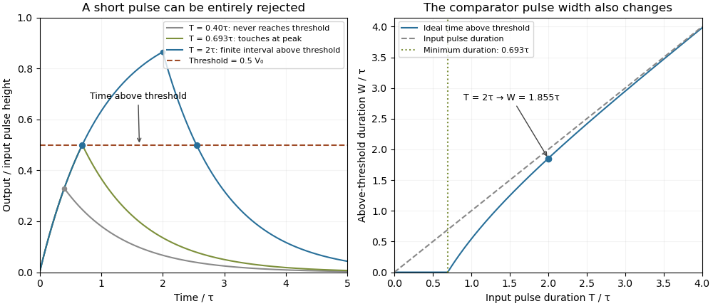

A threshold near the asymptotic input height is also especially sensitive to noise and threshold measurement uncertainty. Holding the absolute input height and fixed, the threshold timing sensitivity of an RC step response isFor the same , model, a effective threshold perturbation gives approximately of timing change at , but at , by first-order uncertainty propagation. The rectangular pulse must still last long enough to reach the selected threshold; changing together with is a different sensitivity calculation.
A bench test uses a pulse generator and an oscilloscope to record both the applied electric potential difference and the capacitor output. Sweep while keeping and the actual threshold fixed, and allow enough time between pulses for the measured initial output to be negligible at the desired precision. Include probe and comparator-input capacitance in . MIT's laboratory measures RC decay with a capacitor, a resistor and square-wave excitation; that gives a directly measurable component-value time constant.[ref]
Laboratory 11: Sinusoidal Steady State Response of RC and RL Circuits by MIT OpenCourseWare. Printed pp. 1–2, component values and decay/phase measurements
The pulse-duration sweep proposed here extends that decay measurement to a threshold observation. A real electronic comparator's input offset voltage, hysteresis and finite switching time must be separated from the ideal RC crossing times; a Schmitt trigger uses different rising and falling thresholds.RC pulse-width discrimination converts an input-duration test into a threshold observation on an RC circuit. For a relaxed first-order load with time constant , a positive rectangular input of height and duration reaches peak output . An ideal electronic comparator has a nonzero interval above fixed threshold precisely whenEquality only touches the threshold at the peak. The parent threshold-crossing time of a finite rectangular pulse through an RC load derives the full response and the rejected-pulse boundary.
This is a duration discriminator only while the input height is controlled. At a fixed duration, the same condition isA larger input can pass the threshold even when a smaller pulse of exactly the same duration fails. The minimum accepted duration decreases with height, with derivative .
For an original example, choose , , and . The minimum height for a nonzero comparator interval is about . A pulse peaks at about and is rejected; a pulse peaks at about and is accepted. Treating this observation as a width-only decision would conflate two different inputs.
A pulse-generator experiment therefore sweeps width at a recorded height and threshold, measures the actual capacitor waveform on an oscilloscope, and allows the initial state to relax. A residual baseline in RC pulse-width discrimination changes the next pulse's peak and invalidates the relaxed-state formula. Probe and comparator input capacitance also belong in the effective time constant. The natural-decay apparatus in MIT's RC laboratory supplies a direct component-level check of that time constant.[ref]
Laboratory 11: Sinusoidal Steady State Response of RC and RL Circuits by MIT OpenCourseWare. Printed pp. 1–2, square-wave decay and sinusoidal measurements
Comparator propagation delay and hysteresis are additional dynamics, not part of the ideal RC acceptance inequality.A capacitor need not finish discharging before the next pulse arrives. This residual baseline in RC pulse-width discrimination changes the next pulse's RC threshold-crossing time even if its applied height and duration are unchanged. The relaxed-state acceptance formula assumes an initial output of zero; a repeated pulse train can violate that assumption systematically.
Take a first-order RC circuit with time constant , input high level , zero input low level and initial capacitor output . During a pulse of duration ,For , solving for the rising threshold givesA finite interval above threshold requires . At equality the output only touches the threshold at its peak. A positive residual makes the crossing earlier than the zero-baseline crossing. If the output already exceeds the threshold at the start, this rising-crossing formula no longer describes a new edge.
The input of a repeated pulse train is a periodic function with high duration , low duration and period . Put and . The next baseline is the previous peak multiplied by . Writing for the baseline before pulse gives the linear recurrence relationBecause , the deviation from its fixed point is a decaying geometric sequence:This periodic RC pulse-train baseline is a repeatable state of the circuit, rather than random readout noise. In the periodic regime, separate rising and falling comparator transitions require . If , there is no finite high interval. If , there is no finite low interval: missing comparator reset in an RC pulse train can turn repeated input pulses into one sustained output state.
For an original calculation, choose , , , and . An isolated relaxed pulse peaks at only and is rejected. The repeatable train instead hasIts rising threshold occurs after each pulse starts. The falling crossing is , giving an above-threshold duration of . Starting from zero baseline, the first three pulses are rejected, but the fourth peaks at and crosses. A change in pulse acceptance need not mean that the source pulse itself changed.
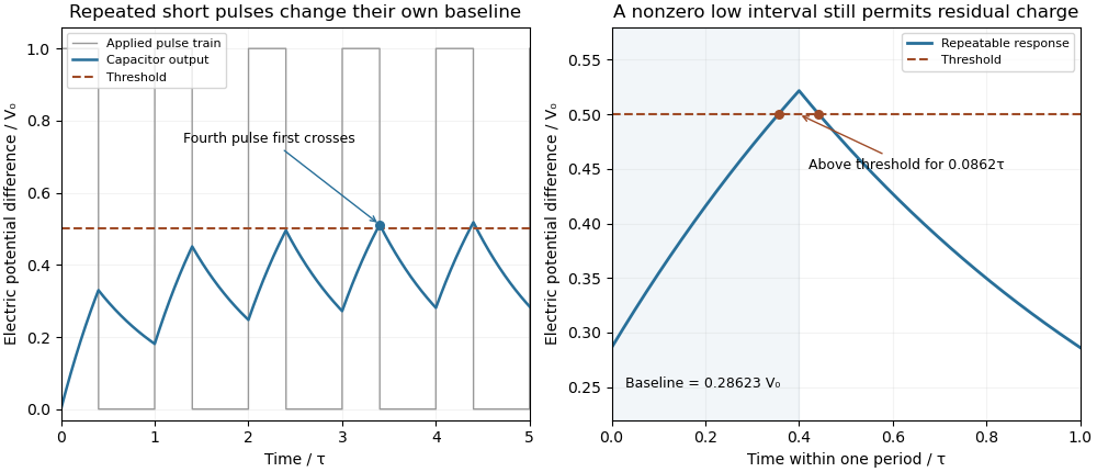
Residual capacitor charge makes a repeated short pulse cross a threshold that rejects the isolated pulse
. Original first-order model, with a 1 µs time constant, 0.4 µs high interval, 0.6 µs low interval and a half-height threshold. The first train starts relaxed; the second panel shows the repeatable baseline and peak. No measured waveforms are used. Details.
A useful design bound controls timing error rather than merely calling the circuit discharged. Put and suppose . Relative to the relaxed crossing,Since a nonnegative pulse train in this model has , a low interval guarantees that baseline bound. Combining the inequalities yields a sufficient quiet interval required for an RC baseline timing budget :For a 1% baseline allowance, limits the crossing advance to , or when . The bound is conservative because it uses the largest possible peak.
A bench test holds pulse height, duration and threshold fixed while sweeping repetition period with a pulse generator. Record the actual input and capacitor output on an oscilloscope, including the baseline immediately before each pulse. Probe capacitance and effective source electrical resistance belong in . MIT's laboratory uses repetitive square-wave excitation to measure RC decay, providing a direct way to check the underlying time constant.[ref]
Laboratory 11: Sinusoidal Steady State Response of RC and RL Circuits by MIT OpenCourseWare. Printed pp. 1–2, natural-response and waveform measurements
The calculations above assume ideal input edges and zero input low level; comparator hysteresis and switching dynamics require their own model.The quiet interval required for an RC baseline timing budget controls how much a residual capacitor baseline may advance the next threshold crossing. In residual baseline in RC pulse-width discrimination, a positive baseline changes the relaxed crossing byFor a permitted advance , requiring is equivalent to , where . To retain a fresh rising crossing, also require , equivalently .
After a previous peak , a zero-input low interval gives . Hence a measured upper bound on that peak gives the sufficient intervalUsing only the model bound recovers the conservative expression in the header, . The peak bound and initial-state assumptions are part of the guarantee. The next pulse must still last long enough to produce the rising crossing; this timing bound alone does not guarantee acceptance.
For an original timing budget, let , and . Then , and the conservative interval is . If a validated peak bound is only , it reduces to . Simply calling either interval several time constants long would hide the actual timing specification.
For , expansion gives under the full-height peak bound. Tightening a small timing allowance by a factor of two therefore adds roughly of quiet time. If the allowed advance is as large as the whole relaxed crossing time, a separate reset condition is still required; the logarithmic timing budget alone no longer ensures the initial output is below threshold.
A bench test measures the peak and the baseline while sweeping the low interval, keeping the threshold and pulse height fixed. MIT's RC laboratory supplies the natural-decay measurement used to check the underlying time constant.[ref]
Laboratory 11: Sinusoidal Steady State Response of RC and RL Circuits by MIT OpenCourseWare. Printed pp. 1–2, repetitive excitation and RC decay
Probe capacitance and source resistance belong in that measured time constant.Missing comparator reset in an RC pulse train occurs when the filtered output never spends a finite interval below the reset threshold between pulses. In the periodic first-order model, with and , the baseline is the minimum output and equalsFor a nonhysteretic ideal electronic comparator with , leaves no finite low interval. At equality the waveform merely touches the threshold. This is different from a pulse whose peak never reaches threshold and therefore gives no finite high interval.
Solving the strict reset condition givesSeparate rising and falling transitions also require the peak to exceed the threshold. Both inequalities matter, so increasing the quiet interval is not automatically sufficient to produce an accepted output pulse from a weak input.
For an original three-regime example, take , , and . The reset boundary is . At , the periodic baseline/peak are about : after startup the electronic comparator does not reset. At , they are , allowing both transitions. At , the peak is only about , so no finite high interval is produced. The same input height and high duration can therefore give three different output patterns as repetition changes.
The threshold-reset margin for a periodic RC pulse train must also accommodate uncertainty and switching dynamics. With a Schmitt trigger, the lower switching threshold controls reset while the upper one controls acceptance. The capacitor-level inequalities alone do not specify propagation delay or a real electronic comparator's minimum switching dwell time.
A test records the source, capacitor output and electronic comparator output together while sweeping . A steady high output with a pulsing input should be compared with the measured capacitor minimum before being attributed to a source failure. The RC decay model can be checked independently using the primary laboratory's natural-response method.[ref]
The threshold-reset margin for a periodic RC pulse train is the separation between the reset threshold of an electronic comparator and the largest baseline that the periodic RC low-pass filter may leave between pulses. A positive margin excludes missing comparator reset in an RC pulse train in the ideal threshold model; its size measures tolerance to additional electric potential difference errors.
Let be the input high level, the high duration, the quiet duration and the time constant. From the periodic solution in missing comparator reset in an RC pulse train, writeThis defines a margin in volts, rather than in units of standard deviation. If a nominal baseline has a known absolute error bound and the reset threshold has bound , a sufficient worst-case condition isThese are simultaneous bounds on the actual baseline and threshold. Adding their standard uncertainties would not by itself provide a deterministic guarantee; a probabilistic statement requires a specified joint probability distribution.[ref]
Guidelines for Evaluating and Expressing the Uncertainty of NIST Measurement Results by Barry N. Taylor and Chris E. Kuyatt. §§6.2–6.3, distributional conditions for interpreting uncertainty intervals
For an original example, let , and . Then , and the peak is . A threshold of gives . Bounds and leave . Raising the baseline bound to would remove this guarantee even though the nominal waveform still crosses the threshold.
A positive minimum separation does not specify the reset dwell time below threshold in an RC pulse train. A real electronic comparator needs enough time to switch, and the peak must separately exceed the acceptance threshold. For a Schmitt trigger, use the lower switching threshold in , while checking the upper one against the peak.
A focused bench test records the pulse generator output, capacitor output and electronic comparator output on an oscilloscope, then varies near the predicted boundary. Compare the measured minimum with the reset threshold and record the low interval as well as the minimum. The underlying exponential decay can be checked by the natural-response experiment in the MIT laboratory; the margin calculation above is an original application of that model.[ref]
Laboratory 11: Sinusoidal Steady State Response of RC and RL Circuits by MIT OpenCourseWare. Printed p. 1, capacitor response after switching and time-constant measurement
The reset dwell time below threshold in an RC pulse train is the continuous time for which the filtered electric potential difference lies below an electronic comparator's threshold between successive accepted pulses. A positive threshold-reset margin for a periodic RC pulse train ensures a crossing in the ideal model, but does not ensure a long enough low interval for the intended electronics.
Consider the periodic RC low-pass filter response to a high level lasting , followed by zero input for a quiet time . Let be the time constant, the periodic baseline at the start of the high interval and the peak at its end. Assume a nonhysteretic ideal electronic comparator and . Solving the two exponential segments gives the rising crossing time , measured from the high interval's start, and the falling crossing delay , measured from its end:The below-threshold interval runs from the falling crossing to the next rising crossing. ThereforeIncluding matters: the low interval usually extends into the next input high interval. The natural exponential decay underlying these segments is directly testable with the switched-RC apparatus in the MIT laboratory.[ref]
Laboratory 11: Sinusoidal Steady State Response of RC and RL Circuits by MIT OpenCourseWare. Printed p. 1, natural-response and time-constant experiment
For an original exact example, take , and . The periodic solution in missing comparator reset in an RC pulse train gives and . At , both crossing delays equal , so . The reset margin is a positive , yet a stipulated requirement of at least low time is not met.
The strict crossing assumptions are essential. At , the waveform only touches the threshold and the low interval vanishes. At or above the peak there is no finite high interval to separate. A Schmitt trigger uses distinct switching thresholds, so its output-state interval requires the corresponding falling and rising crossings rather than substituting one threshold indiscriminately.
A proposed measurement records the pulse generator, capacitor and electronic comparator outputs on an oscilloscope. Measure the low interval between actual output edges while also locating both capacitor-level crossings. Their difference can expose switching delays; the capacitor formula alone does not specify a real device's minimum pulse duration.
A periodic RC pulse-train baseline is the repeatable pre-pulse capacitor voltage reached after startup. It need not be zero even when the input low level is zero. With high duration , low duration , period , and , , the recurrence in residual baseline in RC pulse-width discrimination has contraction factor . Its fixed baseline and peak areThis is a deterministic periodic state, not a random noise floor. The startup error is reduced by a specified fraction after cycles, rounded upward.
The mean supplies an independent check. Integrating over a full period makes the derivative term vanish, so . The mean depends on duty cycle while the baseline and ripple depend on period relative to the time constant. For at fixed , expansion givesThus a rapid train approaches a level near its duty-cycle average, rather than isolated relaxed pulses.
For an original fast-train example, choose , , and . The exact baseline is about , the peak , and the mean exactly . The startup deviation contracts by each cycle; reducing it below one percent of its initial value takes 24 cycles, or .
A pulse-generator/oscilloscope test should therefore distinguish the first pulses from the repeatable train, and record minima, maxima and mean rather than only input width. The natural-response measurement in the primary RC laboratory checks the time constant used here.[ref]
Laboratory 11: Sinusoidal Steady State Response of RC and RL Circuits by MIT OpenCourseWare. Printed pp. 1–2
Threshold placement relative to the repeatable minimum and maximum determines acceptance and missing comparator reset in an RC pulse train.Threshold timing sensitivity of an RC step response measures how a crossing time changes when the absolute threshold or signal height changes. For a relaxed step response , with , the rising crossing isHolding the other inputs fixed givesA threshold approaching the step height encounters a flatter part of the exponential response, making the first sensitivity large.
For an original timing estimate, choose , , and effective small threshold-noise standard deviation . At , local linear propagation gives timing standard deviation about . At , it gives about . The latter threshold also needs a longer input pulse to be reached at all, as shown in threshold-crossing time of a finite rectangular pulse through an RC load.
The two voltage sensitivities can cancel under a different measurement calibration model. If the threshold is set to a fixed fraction of the same varying height, and , their contributions sum to zero. The crossing becomes , independent of amplitude in this ideal model. Such correlated threshold and amplitude errors in RC timing must retain covariance rather than add two independent voltage uncertainties.[ref]
The local noise rule also follows from dividing a small voltage perturbation by the crossing slope . It assumes a well-defined nearby crossing and sufficiently small perturbations; it does not describe multiple noise crossings, comparator switching dynamics, or a pulse ending before the threshold. A bench test can compare controlled threshold shifts with oscilloscope crossing times while holding the actual step height and initial state fixed.
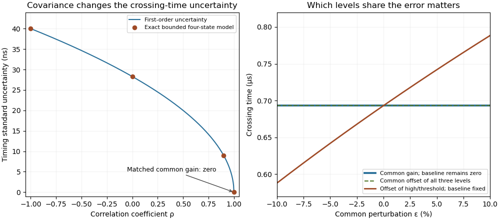
Covariance changes RC timing uncertainty, while gain and offset cancellation depend on the full measurement model
. Original calculation for a 1 V high level, 0.5 V threshold and 1 µs time constant. Exact four-state bounded-error checks are compared with first-order propagation. The right panel distinguishes common gain, a two-level offset with fixed baseline, and a common offset of all three levels. Its common perturbation sets gain or offset . No measured uncertainty data are used. Details.
A common offset in RC timing cancels only when every level used in the crossing model shares the same additive change. For high level , threshold , and initial baseline , assume and fixed time constant . The crossing time isAdding to all three levels leaves both differences unchanged, so the invariance in the header is exact. It describes a shared readout zero, or an equivalently translated step with a translated initial condition, rather than every possible physical offset experiment.
The three sensitivities make the cancellation visible locally:A common random offset has covariance matrix for these three inputs and contributes zero to the propagated timing variance. NIST's primary law retains exactly such covariance terms; setting them to zero would represent another measurement model.[ref]
For an original nonzero-baseline example, take , , and . The crossing is about . Adding to all three levels leaves it exactly unchanged. Adding the same offset only to and while keeping the baseline fixed instead increases it by about . The two-level sensitivity is , predicting to first order.
A calibration test must state whether the initial capacitor output, electronic comparator reference, input level and readout share the offset. Independent threshold errors, uncertainty of the time constant, and baseline memory remain even when this one common component cancels. The full distinction is developed in correlated threshold and amplitude errors in RC timing; a common gain is a separate invariance treated in ratiometric cancellation of RC timing gain errors.
Ratiometric cancellation of RC timing gain errors follows when the same positive gain multiplies every voltage level relevant to a threshold ratio. With zero initial baseline, fixed time constant , high level and threshold ,Replacing by with leaves and the time unchanged. This is an exact invariance, not merely the first-order cancellation of two uncertainty terms. It is a ratiometric measurement property of the specified model.
For an original example, choose , and . The crossing is approximately . Gains and both give the same result when they scale high level and threshold together. A shared readout gain can cancel from the calculated time in the same way; whether a reference also changes the physical circuit must be stated separately.
The mismatch remaining after common RC gain cancellation depends on the relative gains, not their common magnitude. Let the high level use gain and the threshold gain , with . Provided ,In the example, a one-percent relative mismatch delays the crossing by about , compared with from the first-order expression. Thresholds nearer the high level amplify the residual.
A nonzero initial baseline must share the gain too: is unchanged by multiplying all three levels by . Scaling only the high level and threshold against a fixed nonzero baseline is another experiment. Likewise, additive errors follow the conditions in common offset in RC timing, not the two-level scaling rule.
Uncertainty in the time constant, independent threshold error, baseline memory, and failure to reach the threshold remain even when one common gain cancels. Their covariance structure must follow the complete measurement model, as in correlated threshold and amplitude errors in RC timing and NIST's propagation law.[ref]
The mismatch remaining after common RC gain cancellation is the timing error caused by unequal gains in the amplitude and threshold paths after their common multiplicative part has canceled. It depends on their ratio, so improving a shared gain alone does not remove it.
For the zero-baseline RC threshold-crossing time, let with . If the amplitude is multiplied by and the threshold by , define the residual relative error by . The exact result from ratiometric cancellation of RC timing gain errors isHere is the time constant. As approaches one, the crossing is arbitrarily late; at or above one there is no finite rising crossing. An error budget must check this existence condition as well as a small timing residual.
For a new example, set , and . A one-percent positive mismatch gives ; a one-percent negative mismatch gives . The first-order estimate is , or here. The unequal exact magnitudes are a consequence of the logarithm, not an asymmetric tolerance specification.
If , monotonicity gives the exact worst absolute errorThus a bound in this example requires , about . This is a bound on the gain ratio, not on either gain separately.
For small fractional path errors , andA perfectly shared component has zero contribution to that difference. This is the law of propagation of uncertainty applied to the two gains; it does not cancel a change in , an additive threshold error or a nonzero unscaled baseline.[ref]
A proposed check varies the common gain while holding its ratio fixed, then varies only one path. Recording the two electric potential differences and the crossing on an oscilloscope distinguishes the exact common-gain invariance from the surviving mismatch.
The time above threshold for an RC-filtered rectangular pulse is the separation of its rising and falling threshold crossings, rather than the applied pulse duration. In the relaxed first-order model, put with and . The parent crossing calculation givesThis excludes comparator propagation dynamics and uses the same threshold on both edges. A Schmitt trigger with unequal switching thresholds needs a different formula.
The positive-width relation can be inverted exactly:Its derivative is . Thus a measured positive determines a unique input duration under the stated model. A zero-width observation does not: all rejected durations have that same outcome.
For an original example, take , and . The output remains above threshold for about , longer than the input pulse because of its decaying tail. Substitution into the inverse relation recovers .
For long pulses, tends to . It is positive below a half-height threshold and negative above one. At exactly half height, for every finite accepted pulse, with the difference tending to zero for long pulses. Consequently a measured above-threshold width cannot be equated to the input width without the threshold and filter model.
A pulse-generator/oscilloscope comparison can record both widths while varying threshold. The measured RC decay should be checked independently, using the natural-response method in the primary MIT laboratory.[ref]
Laboratory 11: Sinusoidal Steady State Response of RC and RL Circuits by MIT OpenCourseWare. Printed pp. 1–2
Initial residual charge, hysteresis, and different rising/falling comparator delays alter the observation; the algebra above only inverts the ideal capacitor waveform.The ratio of output to input signal electric current, with specified reference directions and load conditions. A large current gain alone does not determine power gain.
The ratio of signal power delivered to a specified output load to signal power accepted at a specified input, with . An amplifier draws additional energy from its supply, so a power gain above one does not create energy.
A lock-in amplifier measures the component of an input signal synchronized with a reference at a chosen frequency. It multiplies the input by a reference sinusoid, then uses a low-pass filter to retain the slowly varying product. Two references in phase quadrature recover both amplitude and phase difference. A shared timing source keeps the relative wave phase stable: this is coherent detection.[ref]
Model SR830 DSP Lock-In Amplifier manual by Stanford Research Systems. Model SR830 DSP Lock-In Amplifier manual, revision 2.5, printed pp. 3-1–3-2: multiplication, filtering, reference locking and dual-phase detection
The useful trick is to move the wanted frequency to zero before averaging. An electronic amplifier alone enlarges both the wanted signal and unwanted noise; a lock-in amplifier instead selects a component by its timing. A photodiode's electric current can first be converted to an electric potential difference, so the same calculation can measure weak modulated light. The chopped-light lock-in experiment makes this selection tangible.
phase-sensitive detection correlates an input with a synchronized reference and filters the product. Sinusoidal quadrature references recover both signal amplitude and relative phase. Narrow detection bandwidth rejects incoherent noise but cannot reject a background coherent at the same frequency; changing the integration time also changes settling and tracking speed.[ref]
Let the input electric potential difference be , with peak amplitude , angular frequency , and phase difference relative to . For an observation interval containing an integer number of cycles, each lasting one period of a function, , define the lock-in quadratures in a peak convention:These integrals average the products with dimensionless references and ; and have the input's units. The minus sign makes positive give positive . The trigonometric functions giveThe oscillating terms have zero integral over the stated interval, proving and . Their orthogonality turns an oscillating signal into two constant coordinates.
Represent those coordinates as a vector, or as the complex number . Its modulus and complex argument recover the peak amplitude and phase difference:Here selects the angle with the correct signs of both coordinates, rather than applying the arctangent to and losing the quadrant. When , the amplitude is zero and the phase difference is undefined. When , despite a nonzero signal; measuring prevents this blind spot. Rotating both references by a fixed angle rotates the coordinate vector but preserves .
The factors of two above deliberately recover peak amplitude. The SR830 instead reports the selected sinusoidal component in root mean square units: in a calibrated, zero-offset display, . For this is , while the peak-to-peak span of that component is . Display normalization, reference sign, gain and angle units must be checked for the particular instrument.[ref]
Model SR830 DSP Lock-In Amplifier manual by Stanford Research Systems. Model SR830 DSP Lock-In Amplifier manual, printed p. 3-3, “RMS or Peak?” and “Degrees or Radians?”; pp. 3-13–3-14, output scaling and display offsets
Consider this original constructed input electric potential difference, with in seconds and :The unwanted component has three times the reference frequency and more than twice the wanted peak amplitude. Nevertheless, the lock-in quadratures over are exactlyso and . This is a peak amplitude calculation, not an SR830 display prediction.
To see why the larger component vanishes, multiply by each reference:Each sinusoid has zero average value of a function over a whole reference cycle. More generally, a component with integer gives products at and , whose integrals vanish over any integer number of reference cycles. This is the orthogonality behind selecting a Fourier coefficient with sinusoidal references. A nonsinusoidal reference can contain additional frequencies and need not have the same rejection property.

An unwanted component at the reference frequency survives. If is added to the input, its coordinate vector adds to the wanted one:For example, adding with to the wanted component gives , , , and phase difference . Longer averaging cannot separate these two synchronized contributions.
An observation interval of finite duration is not an infinitely sharp frequency selector. Combine the lock-in quadratures intoFor unwanted electric potential difference , where is an angular frequency offset and , expansion into complex exponentials gives the exact responseThe sinc function formula follows by integrating the exponential function and factoring ; its value at zero follows from a limit. The first term changes slowly after multiplication; the second oscillates at the sum frequency. It vanishes at exact matching when is an integer number of reference cycles, each lasting one period of a function, but cannot generally be discarded in a short-window calculation.
For and many reference cycles, the first term usually dominates: its modulus is and its complex argument includes . Thus gives almost no rejection. A longer observation separates closer frequencies, with the first zeros of this term at . Those zeros are not a brick-wall cutoff: the sinc function has nonzero lobes beyond them. At a synchronized contribution remains however large becomes.

For a numerical check, use , , and an unwanted frequency . Then and the exact expression giveswhereas the difference-frequency term alone gives . An interference amplitude therefore contributes to in this constructed example. A nearby frequency can survive strongly even though the three-times-frequency component in lock-in harmonic rejection cancels exactly.
A practical lock-in amplifier's low-pass filter weights past products differently from this rectangular observation interval. Its time constant and roll-off determine near-reference rejection and settling time; narrowing detection slows the response.[ref]
Model SR830 DSP Lock-In Amplifier manual by Stanford Research Systems. Model SR830 DSP Lock-In Amplifier manual, printed p. 3-2, “Narrow band detection”; pp. 3-11–3-12, time constants and filter roll-off
The University of California, Berkeley guide LLS - Measuring the Light Signal from a Diode, in Experimental Setup and Experiments X–XI, documents an experiment using a red light-emitting diode amid room-light background. An optical chopper, controlled by an SR540, periodically interrupts its light. A PIN-10DP photodiode sends electric current to an SR570 preamplifier, which converts it to an electric potential difference for an SR760 spectrum analyzer and an SR830 lock-in amplifier. The SR540 supplies the external reference. Preparation includes aligning the photodiode and its shielding cone and choosing gain to avoid overload. One comparison first searches for the source frequency without the chopper reference, then checks against that external reference; switching off the LED tests the candidate spectral peak. The measurement procedure varies chopper frequency and preamplifier filtering, then records repeated lock-in readings with selected averaging settings. These are prescribed observations to make, not published numerical results.[ref]
LLS - Measuring the Light Signal from a Diode, University of California, Berkeley. LLS - Measuring the Light Signal from a Diode, Experimental Setup; Block Diagram I; Experiment X, steps 2 and 9–13; Experiment XI, steps 1–8
The guide notes nearly triangular chopping because slit and emitter sizes are comparable. Its interpretation requires detector conversion, preamplifier gain and waveform geometry to infer optical power from the selected component.[ref]
LLS - Measuring the Light Signal from a Diode, University of California, Berkeley. Experimental Setup, waveform discussion; Interpreting the Data, points 1–3 and collection-geometry discussion
The inference is therefore specific: synchronized electric potential difference supports the presence of a modulated optical component at the reference frequency. It does not by itself give total emitted optical power. The photodiode's spectral responsivity, collected fraction of the light, and conversion from the measured Fourier coefficient to the chopped waveform must enter that calibration. The finite-window lock-in response also explains why a frequency-search reading can drift when the reference is not synchronized. An LED-off comparison tests background at the same timing; it cannot guarantee that every synchronized disturbance disappears when the desired source is present. Overload before multiplication destroys information that later averaging cannot restore.
Articles by others on the same topic
There are currently no matching articles.