A charge-coupled device stores photoelectrons in potential wells and transfers the charge through clocked stages to an output amplifier. The transfer differs from independently addressed pixels in a hybrid infrared detector.
In an imaging charge-coupled device, absorbed photons produce mobile charge carriers in a semiconductor; collection stores an electric charge packet associated with each optical detector pixel. Closely spaced MOS capacitors allow applied electric potential differences to move the packet from site to site. Willard Sterling Boyle and George Elwood Smith described storage, transfer and detection as distinct operations, including imaging as one application.[ref]
Charge Coupled Semiconductor Devices by Willard Sterling Boyle and George Elwood Smith. Charge Coupled Semiconductor Devices, April 1970, p. 587, abstract and opening device-concept paragraphs; scanned original hosted by VTDA
The useful architectural trick is that many optical detector pixels can send their electric charge to a shared output electronic amplifier. This makes repeatable conversion possible but makes fidelity depend on every transfer along the route. An active-pixel sensor made with CMOS technology instead uses circuitry at pixels to convert or buffer their signal and select it for readout; independent pixel addressing does not require transporting each packet through the whole image. This compares readout architectures, not whether either technology can use a photodiode.[ref]
CMOS Sensors Enable Phone Cameras, HD Video by National Aeronautics and Space Administration. NASA Spinoff, 2017, NASA Technology, pixel-to-pixel transfer and amplification at individual pixels
A photon of energy fully absorbed in silicon produces on average electron-hole pairs, with variance rather than necessarily a Poisson variance. Thus and Gaussian FWHM is . Representative silicon values eV and give about eV FWHM at keV. read noise in split-event pixels, trapping and gain errors broaden that limit; optical pixel size alone does not specify the energy resolution.[ref]
The ASCA Data Reduction Guide by NASA HEASARC. §4.7, non-uniform CTI and Fano-limited FWHM expression
For source electrons , sky electrons , dark-current rate , total exposure , reads and rms read noise , independent variances add to . calibration can remove reproducible means but cannot remove the science exposure's random photon or dark-current fluctuations. A finite background estimate and imperfect calibration add further uncertainty.
For total source electrons , aperture pixels, sky-plus-dark rate , time , reads with rms , and an independent mean-background estimate of variance per pixel, the aperture variance is before additional calibration terms. The last factor is because one uncertain background mean is subtracted from all aperture pixels. Pixel correlations require covariance terms.
For an electron packet, a sufficiently positive gate electric potential attracts electrons beneath the insulating layer of a MOS capacitor. The corresponding potential energy is , where is the magnitude of elementary charge: a larger electric potential gives a deeper potential well for electrons. A drawing of potential energy must therefore reverse the vertical sense of a drawing of electric potential.
A simplified three-phase transfer raises the adjacent gate's electric potential before lowering the old holding gate. This overlaps the accessible regions, then leaves the packet under the new gate. Repeat with the next gate to move it forward. Isolated wells with an intervening barrier would store the packet without transferring it.[ref]
Charge Coupled Semiconductor Devices by Willard Sterling Boyle and George Elwood Smith. Boyle and Smith, 1970, p. 587, neighboring capacitors and manipulated electrode potentials
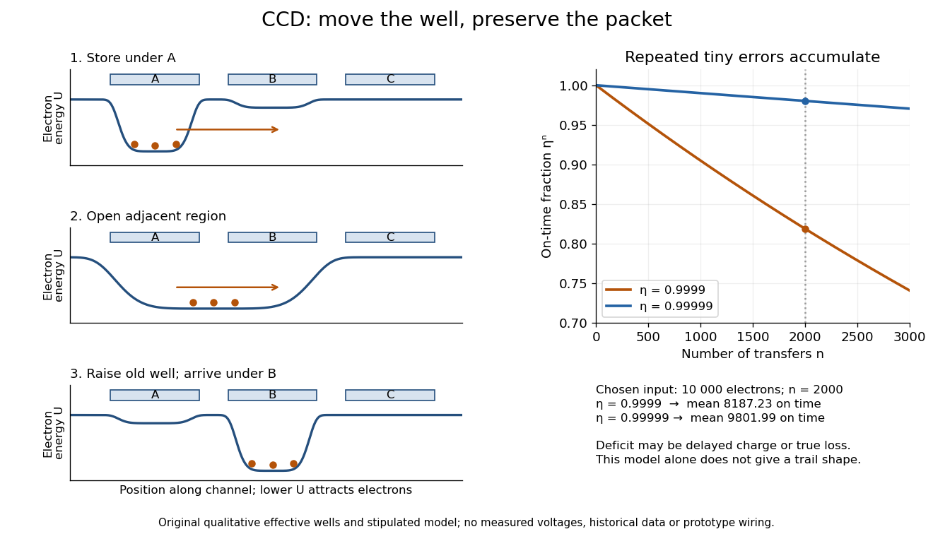
CCD clocked charge transfer and cumulative charge-transfer efficiency
. Original explanatory potential energy profiles show storage, overlap and arrival, with lower curves meaning more attractive regions for electrons. These are qualitative effective profiles, not measured voltages or prototype wiring. The right panel calculates the main-packet fraction for the stipulated constant-efficiency model; charge absent from that packet may be deferred or truly lost. Details.
The charge-transfer efficiency is the fraction of a packet delivered into its intended next site or time slot in one transfer, under stated conditions. It is distinct from quantum efficiency, which concerns conversion of incident photons into collected charge carriers. Define the complementary inefficiency as .
In an original model with constant , let denote the mean number of original packet electrons still delivered on time after transfers. Assuming no reinjection into that packet,Repeated substitution proves the result; for different efficiencies the fraction is . For , a Taylor expansion of gives , while the simpler requires .
Choose and . For , the expected on-time output is electrons; for , it is . These are model means, so fractional electron counts do not describe an individual packet. Even a small per-transfer imperfection can imprint distance-dependent image errors.
If every original electron independently stays on time with probability , a fixed initial count gives a binomial distribution with variance . An initial Poisson distribution with mean instead gives an on-time Poisson distribution with mean and variance , by Poisson thinning. A deterministic attenuation formula alone does not specify noise. Real trapping can correlate packets and depends on timing, illumination and temperature; the independent constant-efficiency model then fails.
Deferred charge in CCD readout reaches later output samples than its originating packet. George Elwood Smith describes surface states at the silicon–silicon dioxide interface capturing electrons and releasing them later, smearing the image. A buried channel keeps the stored packet away from that interface.[ref]
Nobel Lecture: The invention and early history of the CCD by George Elwood Smith. pp. 2310–2311, Figs. 10–11, trapping
An original comparison separates two interpretations of the same main-packet deficit. If a single transfer defers fraction by exactly one sample and loses nothing, an isolated input packet produces samples followed by : summing both recovers . A truly lossy transfer yields only , with no later recovery. For and , both give in the intended sample, but only the deferred case gives a -electron trail. Such a trail redistributes position information even when total electric charge is conserved. Repeated delays require a time-response model; alone cannot predict trail shape. Electron-hole recombination, escape to another contact, or release beyond the recorded window can instead remove signal from the measured sum.
George Elwood Smith reports fabricating MOS capacitors, thermally generating the first packet, and clocking it to an output that pushed it into the substrate for electric current detection. A later integrated eight-bit device demonstrated imaging. Dark or reversed-clock control traces are not specified; feasibility alone does not calibrate charge-transfer efficiency.[ref]
Nobel Lecture: The invention and early history of the CCD by George Elwood Smith. pp. 2309–2310, Figs. 7–9, prototype and imager
A discriminating repeat would compare identical cycles with and without initial carrier injection, then suppress or reverse the transfer sequence while retaining output switching. An electric current transient synchronized with gate switching can include capacitor feedthrough; only the difference tied to initial electric charge and the expected transfer delay tests packet transport. These are proposed controls, not controls documented in the lecture. For an optical version, a blocked exposure estimates dark current and read noise; a spatially isolated illuminated optical detector pixel exposes any deferred charge in CCD readout trail. Photon shot noise persists even with ideal transfer.
An electron-multiplying CCD adds a high-field multiplication register before the output amplifier. Impact ionization generates a large mean gain, reducing input-referred read noise but adding multiplication excess noise.
Random multiplication increases the noise relative to deterministic gain. If the output from one input electron has mean and variance , a Poisson distribution of input electrons with mean produces output variance , by the law of total variance. The high-gain analog-mode excess-noise factor is .
An energetic charge carrier creates an additional electron–hole pair. In a multiplication register this is stochastic, so the output charge fluctuates even when the input electron number is fixed.
For a direct-gap semiconductor with equal parabolic conduction-electron effective masses, restrict the final valence hole to zero crystal momentum and consider a normal process. Momentum conservation gives , while energy conservation gives with . The Cauchy-Schwarz inequality gives , so and the threshold is . Equal final wavevectors attain the bound; opposite spins allow the two electrons to occupy that wavevector. This is the threshold under the stated hole constraint, not the general threshold when the final hole can carry momentum.
Articles by others on the same topic
There are currently no matching articles.