A photodiode is a semiconductor diode producing photocurrent from photon absorption. Exciting an electron across the band gap leaves an electron hole. The depletion region's electric field separates the charge carriers; others can arrive by diffusion before electron-hole recombination. Contacts complete the electrical circuit.[ref]
Si photodiodes by Hamamatsu Photonics K.K.. Si photodiodes, p. 2, §1-1 and Figs. 1-1–1-2: generation, separation and collection
The useful bridge is from light to a measurable electric current: spectral responsivity converts incident radiant flux into photocurrent, while quantum efficiency counts collected signal charge carriers per incident photon. These answer different questions: how much electric current one watt produces, and how many incident photons contribute to the signal. The worked calculation below makes their relationship explicit.
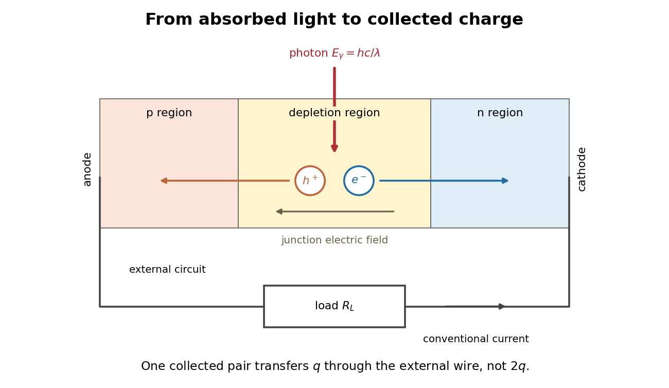
Photon absorption, junction separation and an external electric current
. Original qualitative p-n junction schematic with an external resistor. Collecting one electron–electron hole pair transfers one elementary charge through the external electrical circuit, rather than twice that amount. Dimensions and paths are schematic. Details.
Photodiode saturation is a departure from the intended proportional response of a photodiode as incident radiation becomes too large for the detector's operating conditions. The simple relation , or its pulse-integrated counterpart , then fails with a constant spectral responsivity . The observed readout can also be limited by amplifier clipping or other circuit effects, so a flattened trace alone does not locate the nonlinearity inside the diode.
Robert E. Vest and collaborators characterized silicon-photodiode response under pulsed illumination, reporting dependence on reverse bias and illuminated area. Their study extends pulse-length characterization and compares a pulsed-radiation calibration with continuous-wave conditions at a synchrotron.[ref]
Measuring Pulse Energy With Solid-State Photodiodes by Robert E. Vest and others. Abstract, nonlinear response, bias/area dependence and calibration comparison
Low average optical power does not by itself ensure that an individual pulse remains within the detector's proportional-response range.An original toy response makes the energy bias explicit. Suppose the collected pulse charge isThis chosen compression law is not Vest's detector model. At low pulse energy it approaches ; at high energy it approaches . With , and true , it gives . Blindly applying the low-level calibration would infer50nanojoules, only half the stipulated energy.
A detector linearity test varies incident energy while holding wavelength, illumination geometry, bias and readout settings fixed. In the toy law, halving the true energy from100to50nanojoules changes charge from20toabout13.3nanocoulombs, rather than to10nanocoulombs. Comparing these ratios with known optical changes can expose compression. Actual attenuation and reference measurements require their own measurement calibration.
The appropriate limit depends on pulse shape, area, bias and readout, not on one universal optical-power number. Detector baseline subtraction can correct an additive offset but cannot reconstruct charge lost through an unknown nonlinear response. Establishing linear operation or characterizing that response is therefore a prerequisite for trustworthy pulse energy measurement with a photodiode.
Pulse energy measurement with a photodiode estimates incident laser pulse energy from collected signal electric charge. At fixed wavelength, suppose a photodiode has constant calibrated spectral responsivity in amperes per watt and remains in its linear operating range. If is the incident radiant flux, the signal photocurrent is . Integrating over the complete response givesThe units agree because amperes per watt equal coulombs per joule. Spectral responsivity must apply at the measurement wavelength; a broadband pulse requires accounting for its spectrum.
In an original example, let and let the baseline-corrected collected charge be . Then . An ideal charge amplifier with feedback capacitance would produce an output change of magnitude . The amplifier's polarity depends on its circuit convention.
A practical apparatus needs a calibrated detector, a charge-sensitive readout and a measurement window containing the full response. Detector baseline subtraction removes the estimated background, including dark current. A residual constant current of1microampere integrated over10microseconds contributes10picocoulombs; with the example responsivity this is a25picojoule energy error. Extending the window can capture a missing signal tail but also accumulate more background error.
Photodiode saturation invalidates the assumed constant response. Robert E. Vest and collaborators measured pulsed silicon-detector behavior and reported dependencies on applied reverse bias and illuminated area.[ref]
Measuring Pulse Energy With Solid-State Photodiodes by Robert E. Vest and others. Abstract, nonlinear pulsed response and bias/area dependence
A low average optical power therefore does not by itself establish linear response to individual pulses.Rodney W. Leonhardt's calibration report describes a complementary reference method: a slow thermal standard measures accumulated energy, while pulse count and a calibrated beam splitter ratio determine average energy in the test beam.[ref]
Calibration Service for Low-level Pulsed-Laser Radiometers at 1.06 µm: Pulse Energy and Peak Power by Rodney W. Leonhardt. §4, printed pp9–10
This connects a fast photodiode readout to an energy reference without requiring the thermal standard to resolve every pulse.Collected charge measures energy under the stated assumptions; it does not alone determine peak power. A flat30nanojoule pulse lasting100nanoseconds has power0.30watts, whereas a flat pulse of the same energy lasting1microsecond has power0.030watts. Those stipulated rectangular profiles illustrate why pulse shape and pulse duration are additional information.
A photodiode with a strong internal electric field in which photogenerated charge carriers undergo impact ionization, amplifying the initial signal. Linear multiplication below breakdown and saturated single-event operation above breakdown are distinct operating regimes. A single-photon avalanche diode uses the latter.
A single-photon detector based on a reverse-biased photodiode operated above its breakdown voltage. A carrier generated by photon absorption can trigger a self-sustaining impact ionization avalanche. Quenching lowers the bias to stop that avalanche; recovery creates detector dead time. Random internally generated carriers can also trigger indistinguishable pulses, producing dark counts. Single-photon avalanche diodes ordinarily detect an event rather than resolve the incident photon number. [ref]
https://hub.hamamatsu.com/us/en/ask-an-engineer/detectors/sipm-mppc-spad-questions-and-answers.html. Hamamatsu Photonics, What is SPAD? and How does a SPAD work?: above-breakdown bias and quenching
Subtracting two photocurrents can suppress a shared classical intensity fluctuation when the optical responses and electronic gains are matched. Independent shot noise contributions do not cancel: their variances add in the difference. With equal charge and mean currents , the independent-arrival one-sided current power spectral density is . Correlated optical inputs require their covariance as well.
A photodiode divided into four independently read segments. Differences of opposite segment signals can encode a light distribution's displacement after measurement calibration.
Photocurrent is the electric current attributable to illumination. Here denotes its magnitude after background subtraction. For a photodiode without internal multiplication, let be incident radiant flux concentrated at wavelength , and let be external quantum efficiency, including losses before collection. An incident photon has energy , with Planck constant and speed of light . Dividing energy per second by energy per photon gives the incident photon rate . Multiplying by gives the mean collected pair rate ; multiplying by elementary charge givesThe factor is : each collected pair replenishes an electron at one contact and removes an electron at the other. A cross-section of the external wire therefore counts one transferred electron per completed pair, consistent with charge conservation. The electron and electron hole are two internal charge carriers, not two independent transfers through that wire.
Choose an illustrative photodiode model with , and . Using the exact SI values , and givesA mean fraction does not require each fourth photon to be lost in a repeating pattern. It specifies a mean conversion rate. Nor does mean : quantum efficiency is dimensionless, whereas spectral responsivity compares electric current with power.
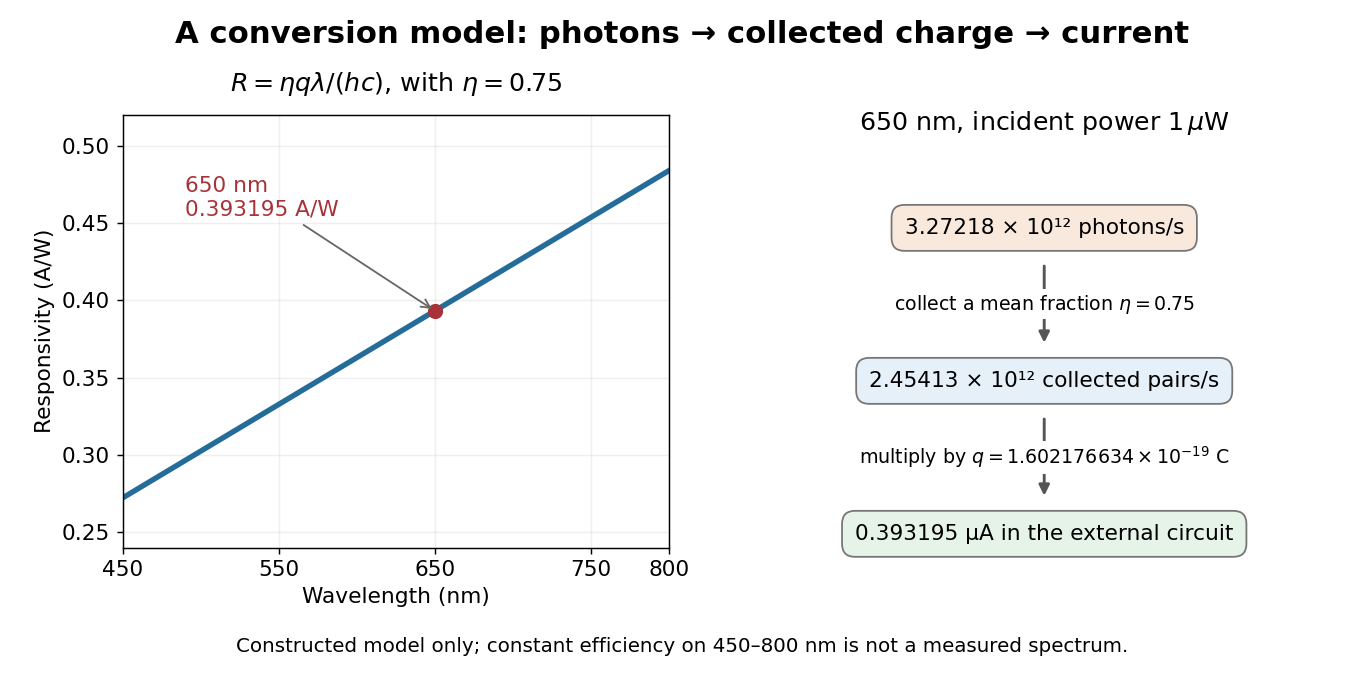

At fixed radiant flux, longer-wavelength photons have less energy, so more arrive per second. This explains the rising straight line when quantum efficiency is held constant. A real photodiode's quantum efficiency varies with wavelength; the plotted assumption cannot be extended past its band gap absorption cutoff. At fixed incident photon rate instead, has no additional factor of .
Photovoltaic mode uses no external reverse bias: a transimpedance amplifier can hold zero terminal electric potential difference, while an open electrical circuit develops a photovoltage. Photoconductive mode biases the diode cathode positive relative to the diode anode, generally reducing junction capacitance and increasing speed and dark current.[ref]
A simple calculation separates the readout from the conversion. If a linear transimpedance amplifier has feedback electrical resistance , the model above produces an output change of magnitude . The output sign depends on the connection. Increasing increases that electric potential difference, but does not create more collected charge carriers.
For a reverse-biased photodiode feeding an electrical load , Ohm's law gives a readout magnitude while the response remains linear. With negligible dark current and other series drops, the remaining reverse bias is , where is the supply magnitude. Thus the chosen electrical load can consume the available bias: a larger readout does not automatically reduce measurement uncertainty. For the same constructed example, and leave about ; this algebra alone does not establish a real device's linear range.
Thorlabs' silicon FDS100 experiment sends a collimated, fibre-coupled laser beam through a beam splitter to the photodiode and a reference optical power meter. Varying reverse bias and electrical load tests linearity. The measured readout approaches saturation when its electric potential difference consumes the bias.[ref]
Photodiodes by Thorlabs. Photodiodes, Lab Facts, Photodiode Saturation Limit and Noise Floor, opening experiment description and Figs. 1–3: reference power sensor, bias/load comparisons and saturation
A separate low-signal setup uses a laser, polarizers, an optical chopper, optical attenuators and a lock-in amplifier inside a light-tight enclosure. These are actual apparatus choices, not the parameters of the constructed example above.[ref]Photodiode Saturation and Noise Floor by Thorlabs. Photodiode Saturation and Noise Floor, p. 7 of 12, Experimental Design — Noise Floor: 637 nm source, polarizers, chopper, attenuation filters, lock-in readout and light-tight enclosure
For an independent dark current check, Thorlabs enclosed a photodiode in nested metal boxes to exclude light and suppress interference, used a Keithley 6487 ammeter supplying reverse bias, and monitored temperature. Only one specimen per type was tested; the nearby temperature sensor did not directly contact the semiconductor. Such a dark control measures the baseline but cannot certify spectral responsivity.[ref]
Photodiodes by Thorlabs. Photodiodes, Lab Facts, Dark Current as a Function of Temperature, Experimental Setup and Experimental Limitations: nested enclosure, ammeter and specimen/temperature limitations
To infer spectral responsivity at a selected wavelength, measure the radiant flux actually reaching the test photodiode, rather than just the reference arm. A reference-arm measurement calibration must include the beam splitter ratio and path losses. With signed readouts in one fixed orientation, subtract a beam-blocked baseline and usefor direct electric current readout or a calibrated linear transimpedance amplifier, respectively. Repeating at several incident powers tests whether this ratio is constant. Blocking only the source estimates ambient light plus electronic baseline; covering the detector excludes ambient light too. Their difference distinguishes optical background from dark current and readout offset. For a broad optical spectrum, the ratio is a spectrum-weighted response, not generally at one wavelength.
For independent Poisson distribution collection, the root mean square shot noise in a one-sided rectangular frequency band of signal bandwidth isHere is reverse dark current; thermal electrical noise and amplifier noise also contribute.[ref]
Si photodiodes by Hamamatsu Photonics K.K.. Si photodiodes, p. 6, §2-4, equations (2-4)–(2-7): independent thermal, dark-current and photocurrent noise terms
Subtracting a mean dark current removes its offset, not its fluctuations: subtracting a constant leaves the variance unchanged. Consequently makes dark current shot noise small relative to signal shot noise; it does not by itself establish high signal-to-noise ratio. With an independently measured baseline, the variance of that estimate must also be propagated. Increasing the measurement signal bandwidth raises the admitted noise. Calibration of wavelength, reference radiant flux, readout gain and collection geometry, together with drift and linearity, determines what measurement uncertainty can be claimed.
Articles by others on the same topic
There are currently no matching articles.