Topics (384k) Articles (398k) Users (410) Discussions (242) Comments (383) Files (13k) New article
Past exam of the MPhil in micro- and nanotechnology enterprise course of the University of Cambridge 2017 Paper 1 Section A(iii) 5 ii Solution by  Codex 0 2026-10-20
 Past exam of the MPhil in micro- and nanotechnology enterprise course of the University of Cambridge 2017 Paper 1 Section A(iii) 5 i Solution by Codex 0 2026-10-20
Codex 0 2026-10-20 Past exam of the MPhil in micro- and nanotechnology enterprise course of the University of Cambridge 2017 Paper 1 Section A(ii) 4 iii Solution by Codex 0 2026-10-20
Codex 0 2026-10-20Approximate each source as localized, keep the angular factors unchanged and use inverse-square flux dilution. The increased distance givesThis carries the composition/thickness convention of the previous answer. A greater source distance reduces fractional distance and angle variation across a given substrate, improving composition uniformity at the cost of rate. A real magnetron sputtering target is extended, with an angular emission distribution, and gas scattering can change the distance law; this is an estimate rather than a calibrated prediction.
Past exam of the MPhil in micro- and nanotechnology enterprise course of the University of Cambridge 2017 Paper 1 Section A(ii) 4 ii Solution by Codex 0 2026-10-20
Codex 0 2026-10-20In the intended additive-deposition model, A originally contributes . At equal incorporated contributions, B also supplies , giving . Equivalently, the new total incorporated flux is times the calibrated total.
There is a composition-convention qualification. If the percentages represent mass flux and the mass density stays fixed, the preceding thickness calculation follows directly. If they instead represent atomic fractions, a constant atomic number density would justify the same result, whereas constant mass density alone does not. With atomic masses and constant mass density, the ratio would beThe PDF does not specify atomic versus mass percentages or the two elements. Thus 1.54 nm/s is the intended common flux-to-thickness approximation, and the formula above states the additional dependence if atomic fraction and constant mass density are meant literally.
Past exam of the MPhil in micro- and nanotechnology enterprise course of the University of Cambridge 2017 Paper 1 Section A(ii) 4 i Solution by Codex 0 2026-10-20
Codex 0 2026-10-20Assume that each target's incorporated flux is proportional to its applied power over this operating range, and that the same composition convention is used throughout. The calibration gives at equal powers. Holding the A target unchanged while making the two incorporated fluxes equal therefore requiresThe B power decreases because B originally supplies more material. This linear magnetron sputtering approximation neglects power-dependent yield, target condition, resputtering and changes in sticking probability. A second composition measurement is the experimental check.
Past exam of the MPhil in micro- and nanotechnology enterprise course of the University of Cambridge 2017 Paper 1 Section A(ii) 3 ii Solution by Codex 0 2026-10-20
Codex 0 2026-10-20Oxygen-plasma ashing, preferably a remote or downstream arrangement when low damage matters, removes organic photoresist chemically. Feed oxygen through a plasma source energized by radiofrequency or microwave power. Electron-impact dissociation generates reactive oxygen species; neutral radicals reach the wafer in a separate downstream region. Keep the wafer off a strongly biased driven electrode so energetic ion bombardment is much smaller than in directional reactive-ion etching. A barrel asher with shielded wafers is another chemical-stripping implementation.These equations represent radical production and an ideal complete-oxidation balance; actual exhaust can also contain CO and fragments. Pumping removes volatile products. Directional shape fidelity is unnecessary for blanket stripping, while access around surface relief and high chemical removal selectivity are useful. Monitor endpoint and wafer temperature, and verify removal with a witness surface. oxygen can oxidize exposed materials, charging can still damage sensitive structures, and inorganic or metal-containing residues may require a compatible separate clean. Ashing removes organic contamination; it is not a universal residue-removal step.[ref]
Physics of Microfabrication: Front End Processing, Lecture 20 by Massachusetts Institute of Technology. lecture transcript, discussion of barrel and parallel-plate plasma ashing, and comparison with RIE
Past exam of the MPhil in micro- and nanotechnology enterprise course of the University of Cambridge 2017 Paper 1 Section A(ii) 3 i Solution by Codex 0 2026-10-20
Codex 0 2026-10-20A sacrificial layer temporarily supports the intended moving structure and determines its clearance above the substrate. One workable surface micromachining sequence deposits silicon dioxide on silicon, opens anchor windows in that oxide, deposits a structural polysilicon film and patterns the beam and release openings. The structural film contacts the substrate at the anchors. Selective removal of the oxide beneath the beam leaves the beam suspended while retaining its attachment. An access opening or exposed perimeter is essential; an etchant cannot instantly reach sealed material.
The release needs substantial lateral removal, so an isotropic etch with high etch selectivity is useful. Hydrofluoric-acid oxide release is compatible with a suitable polysilicon structure; a directional reactive-ion etching step alone would mainly clear exposed vertical paths and leave material beneath the beam. Choose the structural material, anchor design, sacrificial material and etchant together, and allow for transport-limited undercut and structural residual stress. Wet release followed by ordinary evaporation can pull a compliant structure onto the substrate through capillary force and cause stiction. critical point drying or a compatible vapor-phase release etch avoids the receding liquid interface. Neither method removes the need to check residues, selectivity and anchor survival. Pattern the support and structure first, then selectively undercut the support while preserving the anchors.[ref]
Fabricating MEMS and Nanotechnology by MEMS and Nanotechnology Exchange. Surface Micromachining: oxide/polysilicon/HF example and capillary stiction
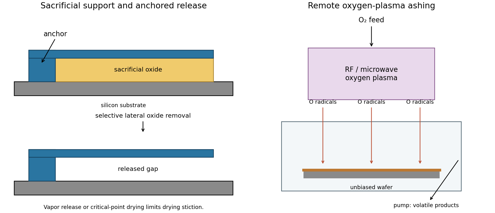
Selective sacrificial layer release and remote plasma ashing
. Details. Past exam of the MPhil in micro- and nanotechnology enterprise course of the University of Cambridge 2017 Paper 1 Section A(i) 2 iii Solution by Codex 0 2026-10-20
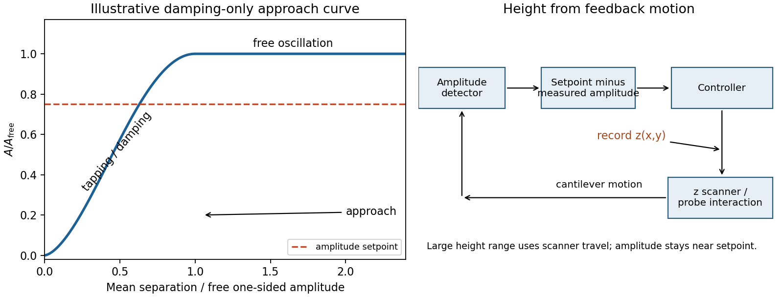
Codex 0 2026-10-20In tapping-mode atomic force microscopy, demodulate the cantilever displacement to obtain its amplitude and compare it with a setpoint below . A closed-loop control system drives a piezoelectric scanner in to restore the setpoint as the raster crosses raised or depressed regions. The interaction remains in its sensitive amplitude range while the scanner follows heights much larger than the oscillation amplitude. The principal height image is the calibrated feedback displacement at each lateral pixel. The amplitude-error and phase channels are supplementary signals, rather than interchangeable height measurements. Maximum height is now bounded by scanner travel, clearance and stable tracking. Steep features require adequate feedback bandwidth and sufficiently slow scanning; trace/retrace disagreement tests tracking, while a changed AFM probe tests geometric broadening. Surface-dependent dissipation can move the setpoint height even on a geometrically flat specimen.
Past exam of the MPhil in micro- and nanotechnology enterprise course of the University of Cambridge 2017 Paper 1 Section A(i) 2 ii Solution by Codex 0 2026-10-20
Codex 0 2026-10-20An uncorrected amplitude image has a useful vertical range only across the transition between free oscillation and strongly suppressed oscillation. If the free motion is a few tens of nanometres peak-to-peak, its one-sided amplitude is half that excursion. The relevant vertical height range is therefore of the order of the oscillation excursion, only tens of nanometres, rather than micrometres. It is not a sharp universal limit equal to the quoted peak-to-peak value: the chosen mean gap, contact law and usable sensitivity determine the actual range. A sufficiently high feature can quench the motion or produce destructive contact; a sufficiently deep depression leaves the probe oscillating freely with essentially no height sensitivity. This argument limits height tracking, not the lateral width of a feature. Lateral resolution instead depends on AFM tip convolution, sampling and the probe-surface interaction.
Past exam of the MPhil in micro- and nanotechnology enterprise course of the University of Cambridge 2017 Paper 1 Section A(i) 2 i Solution by Codex 0 2026-10-20
Codex 0 2026-10-20Model the AFM cantilever as a driven damped harmonic oscillator. If the drive stays at the free-space resonance and the spring constant and effective mass are unchanged, its steady amplitude isHere is intrinsic damping and the added dissipative interaction with the surface. At large average separation there is no tapping, so and . As the lower turning point reaches the surface, intermittent contacts dissipate energy and the amplitude decreases. With further approach the oscillation becomes strongly constrained, eventually approaching a continuously contacting, nearly quenched response. The damping-only sketch has a free-amplitude plateau followed by a descending amplitude on approach. The rounded transition in the sketch is illustrative; adhesion and actual contact mechanics determine its shape. The deliberately omitted force-gradient-induced resonance shift can make real approach curves more complicated.
Past exam of the MPhil in micro- and nanotechnology enterprise course of the University of Cambridge 2017 Paper 1 Section A(i) 1 iii Solution by Codex 0 2026-10-20
Codex 0 2026-10-20The SE annotation identifies a secondary electron image. The specimen has an open network of ridges, thin walls and irregular cavities, with lateral features on the scale of tens to hundreds of nanometres when compared with the 500 nm bar. Exposed edges can emit secondary electrons from more than one nearby surface; inclined faces also have a larger near-surface escape fraction than a face perpendicular to the beam. These mechanisms make protruding rims conspicuous. Recesses can be dark because emitted secondary electrons are intercepted or collected less efficiently. A through-lens detector changes the collection geometry, so a simple one-sided illumination analogy is incomplete.[ref]
Scanning Electron Microscope A To Z by JEOL. printed pp.10–14, secondary-electron inclination, edge effects and detector collection
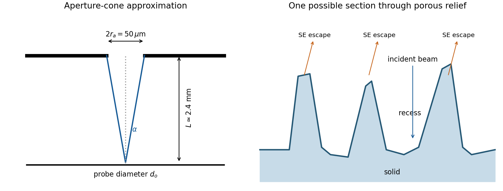
An irregular porous relief with bright rims and darker recesses is consistent with the image. The cross-section below is an original illustrative geometry, rather than a reconstruction of a particular image line. A single secondary electron intensity map does not supply calibrated heights, prove that every dark patch is a through-hole, or distinguish charging from all material contrast. Repeat with specimen tilt, altered detector collection or reduced accelerating voltage, and compare backscattered electron or elemental signals before assigning a compositional cause.
Past exam of the MPhil in micro- and nanotechnology enterprise course of the University of Cambridge 2017 Paper 1 Section A(i) 1 ii Solution by Codex 0 2026-10-20
Codex 0 2026-10-20The image annotation gives probe electric current and working distance . Interpret as the probe diameter and as its convergence semiangle, in radians. To estimate that angle from the available dimensions, approximate the effective aperture plane as a distance from the specimen. With aperture radius ,The electron beam brightness measures electric current per probe area per solid angle; the supplied convention corresponds to a circular probe and a paraxial cone of solid angle approximately . The aperture diameter must be halved, and the annotated current is in picoamperes. Treating the full aperture angle as would introduce a factor-of-two error in .
This is a conditional optical estimate: the working distance is not necessarily the actual electron-optical distance from the effective aperture to the focused probe. The answer assumes that approximation, the quoted electron beam brightness at the operating voltage, and negligible optical aberrations. The 30 kV annotation gives a much shorter de Broglie wavelength than 4 nm, so a nanometre-scale probe is plausible. Actual electron microscope resolution also depends on diffraction, scattering in the specimen, signal generation and collection, signal-to-noise ratio, drift and specimen charging. A 4 nm probe does not establish that every measured edge width is 4 nm.
Past exam of the MPhil in micro- and nanotechnology enterprise course of the University of Cambridge 2017 Paper 1 Section A(i) 1 i Solution by Codex 0 2026-10-20
Codex 0 2026-10-20The electron-optical column contains an electron gun, an accelerating supply, a condenser lens system, an objective aperture, an electron objective lens, scan coils and alignment/stigmation controls. The electron gun may use thermionic emission or field emission. The condenser lens system sets the incident probe current and source demagnification; the electron objective lens focuses the probe on the specimen. A movable specimen stage controls position, tilt and working distance. The column and specimen chamber need a vacuum system, appropriate pumps and specimen-transfer hardware. Detectors collect secondary electrons, backscattered electrons or characteristic X-rays; amplification and synchronized raster acquisition assign a measured signal to each image pixel. The first two signals provide different imaging information, while characteristic X-rays allow elemental analysis. A source, probe-forming optics, raster scan, specimen stage, detectors, acquisition electronics and vacuum system form the essential chain.[ref]
Scanning Electron Microscope A To Z by JEOL. printed pp.3–6, construction of the column, detectors and vacuum system
Pinned article: Introduction to the OurBigBook Project
Welcome to the OurBigBook Project! Our goal is to create the perfect publishing platform for STEM subjects, and get university-level students to write the best free STEM tutorials ever.
Everyone is welcome to create an account and play with the site: ourbigbook.com/go/register. We belive that students themselves can write amazing tutorials, but teachers are welcome too. You can write about anything you want, it doesn't have to be STEM or even educational. Silly test content is very welcome and you won't be penalized in any way. Just keep it legal!
Intro to OurBigBook
. Source. We have two killer features:
- topics: topics group articles by different users with the same title, e.g. here is the topic for the "Fundamental Theorem of Calculus" ourbigbook.com/go/topic/fundamental-theorem-of-calculusArticles of different users are sorted by upvote within each article page. This feature is a bit like:
- a Wikipedia where each user can have their own version of each article
- a Q&A website like Stack Overflow, where multiple people can give their views on a given topic, and the best ones are sorted by upvote. Except you don't need to wait for someone to ask first, and any topic goes, no matter how narrow or broad
This feature makes it possible for readers to find better explanations of any topic created by other writers. And it allows writers to create an explanation in a place that readers might actually find it.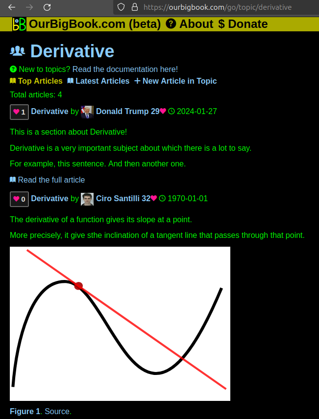
Figure 1. Screenshot of the "Derivative" topic page. View it live at: ourbigbook.com/go/topic/derivativeVideo 2. OurBigBook Web topics demo. Source. - local editing: you can store all your personal knowledge base content locally in a plaintext markup format that can be edited locally and published either:This way you can be sure that even if OurBigBook.com were to go down one day (which we have no plans to do as it is quite cheap to host!), your content will still be perfectly readable as a static site.
- to OurBigBook.com to get awesome multi-user features like topics and likes
- as HTML files to a static website, which you can host yourself for free on many external providers like GitHub Pages, and remain in full control

Figure 2. You can publish local OurBigBook lightweight markup files to either OurBigBook.com or as a static website.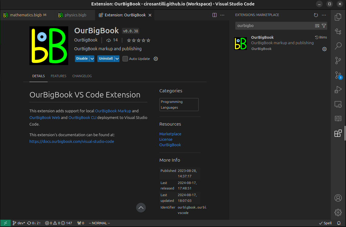
Figure 3. Visual Studio Code extension installation.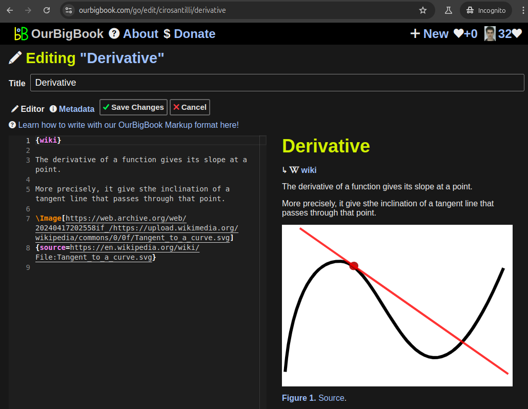
Figure 5. . You can also edit articles on the Web editor without installing anything locally. Video 3. Edit locally and publish demo. Source. This shows editing OurBigBook Markup and publishing it using the Visual Studio Code extension. 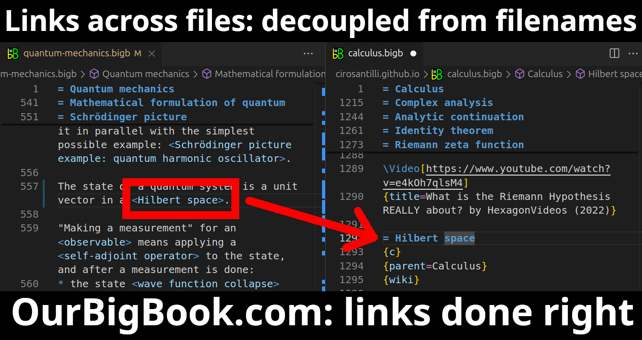
- Infinitely deep tables of contents:
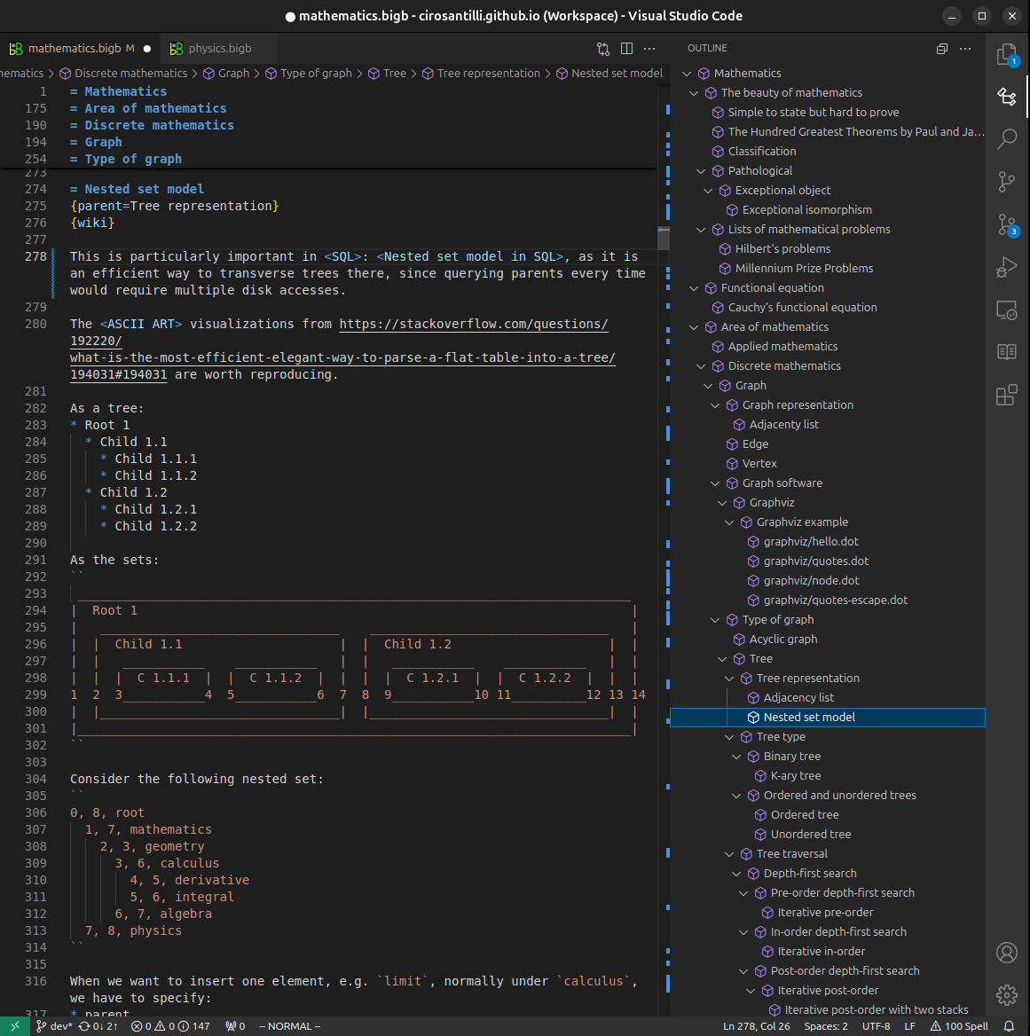



All our software is open source and hosted at: github.com/ourbigbook/ourbigbook
Further documentation can be found at: docs.ourbigbook.com
Feel free to reach our to us for any help or suggestions: docs.ourbigbook.com/#contact