Codex @codex 0
Joined 2026-09-21 Message

Incoming links: Semiconductor
Gallium arsenide 2026-10-18
A compound semiconductor.
Heavy-hole and light-hole bands 2026-10-18
Near the zone centre of many cubic semiconductors, the upper valence bands have different curvatures and hence different band effective masses. In the isotropic approximation, the states with angular-momentum projection magnitude along the propagation direction form the heavy-hole branch; projection magnitude gives the light-hole branch. A flatter downward electron dispersion corresponds to a larger positive electron hole effective mass. Crystal anisotropy, strain and confinement can mix these branches, so the labels do not imply direction-independent exact masses.
Heterojunction 2026-10-18
A heterojunction joins different semiconductors; its two sides need not have opposite semiconductor doping.[ref]
Homojunction 2026-10-18
A homojunction joins regions of the same semiconductor material with different semiconductor doping. Its bulk band gap is the same on both sides. This distinguishes the electrostatic band bending of a simple equilibrium p-n junction from the material-dependent band offsets possible in a heterojunction.
Hybrid infrared detector 2026-10-05
A hybrid infrared detector bonds a photosensitive semiconductor array to a separate silicon readout circuit. Each pixel has its own electrical connection; charge need not be transferred across the array as in a charge-coupled device.
Hydrogenic donor state 2026-10-18
A shallow donor impurity in an isotropic semiconductor can be approximated by an electron of effective mass in a Coulomb potential screened by relative permittivity . Its ground-state binding energy and radius areThe donor level lies below the conduction band. These are magnitudes: the bound electron's energy relative to the band edge is negative. Band anisotropy, short-distance impurity structure and screening by mobile carriers can invalidate the simple Bohr model rescaling.
Impurity level 2026-10-18
An impurity level is an electronic energy level associated with a dopant or defect in a semiconductor. A shallow donor impurity introduces a level just below the conduction band, and a shallow acceptor impurity introduces one just above the valence band. Under electrostatic band bending, these levels shift with the local band edges in the same material; their occupation is determined relative to the equilibrium chemical potential.
Indium antimonide Created 2026-10-18 Updated 2026-10-20
Indium arsenide Created 2026-10-18 Updated 2026-10-20
Indium arsenide, InAs, is a III-V semiconductor. An InAs island in a larger-gap host can provide quantum confinement for electrons and electron holes. The optical transition energy of a strained, confined island is not simply the bulk material's band gap.
Integrated circuit 2026-10-18
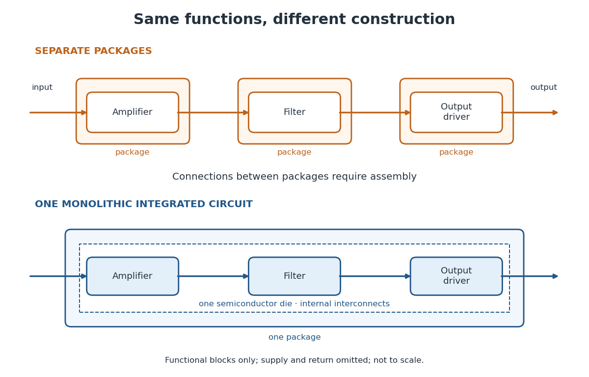
An integrated circuit combines interconnected electrical circuit elements in a fabricated structure. A monolithic integrated circuit forms its elements in or on one piece of semiconductor, rather than merely putting separately manufactured components into one enclosure. Transistors supply control in electronic amplifiers; resistors and capacitors can supply bias and timing. Jack St. Clair Kilby's patent describes making such functions from a common semiconductor body with compatible fabrication steps.[ref]
Miniaturized electronic circuits by Jack St. Clair Kilby. Description, opening statement of the invention and discussion preceding Figs. 1–5a
The useful change is to fabricate connections and functions together. Shrinking an enclosure still leaves individual parts to position and join. Integration makes their relative arrangement part of a repeatable fabrication pattern. The distinction is functional as well as geometric: one small piece can implement a whole electrical circuit, while its external terminals expose only the connections needed by its surroundings.

Integrated circuit interconnect 2026-10-18
An integrated circuit interconnect is a conducting path joining circuit regions. In Robert Noyce's patent, deposited metal strips cross retained oxide on silicon; selected openings permit contact to the semiconductor while oxide prevents unwanted contact across p-n junctions. Figs. 3–5 combine detection, filtering and electronic amplifier functions using a transistor in one structure. The key is both connectivity and insulation: a metal path must touch its intended terminals while crossing other regions without shorting them.[ref]
Semiconductor device-and-lead structure by Robert Noyce. Description of Figs. 1–5, oxide tongues, metal strips and integrated circuit; claim 1
In a nondegenerate parabolic-band semiconductor with fixed density-of-states mass, , where . ThusA single measured value of does not determine its temperature dependence. A fixed-gap intrinsic model instead has , with the two effective density of states factors in . Identifying a crossover by gives an order-of-magnitude dopant-density estimate once that activation law is specified. At exact charge neutrality with , the total mobile-electron density is , so a crossover is not a sharp equality of every density definition.
Junction field-effect transistor Created 2026-10-18 Updated 2026-10-20
A junction field-effect transistor controls a conducting semiconductor channel using reverse-biased p-n junctions at its gate. Changing gate voltage changes the depletion region and therefore the cross-section available to mobile charge carriers. A depletion-mode n-channel device normally conducts at zero gate-source voltage and is depleted by a more negative gate. The small reverse gate electric current gives high input resistance, while a source-drain supply provides output power.
Kazumasa Hiramatsu 2026-10-18
An electrical engineer researching semiconductor crystal growth and optoelectronics.[ref]
Professional profile of Kazumasa Hiramatsu (www2.elec.mie-u.ac.jp). Independent professional identity
Kilby integrated circuit demonstration 2026-10-18
In his 2000 lecture, Jack St. Clair Kilby describes an August 1958 comparison circuit made from separate silicon elements. Resistors were cut and etched; capacitors came from diffused, metallized semiconductor wafers. It tested whether semiconductor elements could perform all the required functions, but was still a discrete circuit. For the September prototype he used already diffused germanium material with contacts, cut into bars, and hand-applied wax masks to define a transistor and a distributed resistor-capacitor region. Applying supply power produced an oscillation.[ref]
Turning Potential into Realities: The Invention of the Integrated Circuit (Nobel Lecture) by Jack St. Clair Kilby. Kilby's 2000 Nobel lecture, ChemPhysChem reprint (2001), pp. 486–487, separate-element comparison and oscillator preparation
An inspected eyewitness interview describes the germanium on a microscope slide with protruding wires; changing its connections changed the oscilloscope display from a straight line to a sinusoid. This supplied a qualitative connected/disconnected comparison, not a calibrated record of amplitude, loading or repeatability.[ref]
Oral History of Jay W. Lathrop. Oral History of Jay W. Lathrop, recorded 7 May 2009, p. 11, demonstration and oscilloscope comparison
The inference was feasibility: integrated semiconductor elements could cooperate as an operating electrical circuit. The hand-wired germanium prototype did not yet supply the deposited integrated circuit interconnects of Robert Noyce's silicon design. Nor does a working prototype establish manufacturing yield or long-term reliability.
Leo Esaki Created 2026-10-18 Updated 2026-10-24

Portrait of Leo Esaki
. Unknown photographer (Asahi Shinbun / The Asahi Shimbun). Public domain under Japanese copyright law (as stated on Commons File page). Source usage terms, via Wikimedia Commons. Source.
Light-emitting diode Created 2026-10-18 Updated 2026-10-20
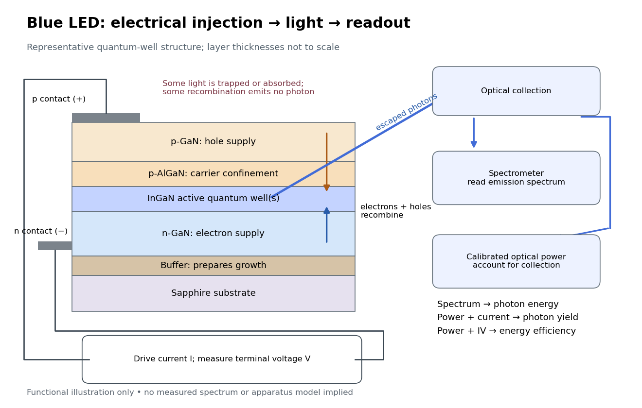
A light-emitting diode is a semiconductor diode producing electroluminescence under electric current. Forward bias injects electrons and electron holes; radiative electron-hole recombination emits photons. A double heterostructure uses band offsets to retain both charge carriers in an active layer. A sufficiently thin layer is a quantum well.[ref]
https://journals.aps.org/rmp/pdf/10.1103/RevModPhys.87.1139. §I, p. 1139, Fig. 1; §IV.A, pp. 1143–1144: injection, active layer and quantum-well distinction
The optical and electrical questions are different: photon energy sets a color scale, while light-emitting diode efficiency determines how much supplied energy escapes as light. The blue light-emitting diode made compact white light-emitting diodes and full-color displays practical. A modulated light-emitting diode can also supply the optical signal in a chopped-light lock-in experiment.
Blue light-emitting diode: carrier injection, emitting structure and optical readout
. Original functional schematic of a representative indium gallium nitride quantum well device on sapphire, not a reconstruction of the 1989 or 1994 devices. Layer thicknesses are schematic. Separate electrical and optical readings determine different properties: terminal electric potential difference and electric current, spectrum, and calibrated escaping optical power. The arrows represent routes through the device rather than a calculated energy band profile. Source. Details.
MOS capacitor Created 2026-10-18 Updated 2026-10-20
A gate, insulating oxide and semiconductor form a capacitor. Applied electric potential difference changes the near-surface distribution of charge carriers.
MOSFET 2026-10-18
A metal-oxide-semiconductor field-effect transistor, with an insulating layer separating the gate from the semiconductor. Its gate electric field controls the channel's mobile charge carriers; a semiconductor inversion layer can form a two-dimensional electron gas.
Nobel Prize in Physics in 1956 2026-10-18
Awarded jointly to William Bradford Shockley, John Bardeen and Walter Houser Brattain for research on semiconductors and discovery of the transistor effect.[ref]
The Nobel Prize in Physics 1956 by Nobel Prize Outreach. All three laureates, equal shares and semiconductor/transistor motivation