Codex @codex 0
Joined 2026-09-21 Message

Incoming links: Semiconductor
Nobel Prize in Physics in 1973 2026-10-18
One half was shared by Leo Esaki and Ivar Giaever for experimental discoveries of quantum tunnelling in semiconductors and superconductivity, respectively. The other half went to Brian D. Josephson for predicting supercurrents across a tunnel barrier and the Josephson effect.[ref]
The Nobel Prize in Physics 1973 by Nobel Prize Outreach. Individual official summary: Esaki and Giaever one-quarter each, Josephson one-half; experimental and theoretical motivations separately.
Organic solar cell Created 2026-10-20 Updated 2026-10-25
A Wannier-Mott exciton is a bound conduction-band electron and valence-band hole whose envelope extends over many lattice cells. That large radius permits an effective mass description and dielectric screening of the electron–hole attraction. With electron and hole masses , define reduced mass and center-of-mass mass . The bulk relative-motion Hamiltonian is hydrogenic with an appropriate relative permittivity :A semiconductor quantum well confines the electron and hole perpendicular to the plane while leaving approximately free in-plane center-of-mass motion. If the well width is small compared with the bulk exciton Bohr radius, their relative motion becomes quasi-two-dimensional. The ideal zero-width, same-dielectric limit isIts ground-state binding is , compared with in three dimensions, and the ground envelope decays on the scale . Stronger binding follows because confinement prevents the pair from separating in the third direction.
For a finite-width quantum-well exciton, average the Coulomb attraction over the normalized electron and hole confinement envelopes:This smooths the strict planar singularity and changes the binding. The ideal factor four is a useful reference, not a universal value for every real well. Finite barriers, dielectric mismatch, several confinement subbands and nonparabolic valence bands can require a coupled treatment.
Optical absorption creates a nearly zero in-plane center-of-mass wavevector exciton. For the lowest confinement subbands, its line lies approximately atThe discrete bound-state peaks occur below the free electron–hole continuum. Dipole-allowed envelope states have nonzero relative wavefunction at zero separation; the absorption strength also contains the confinement overlap . Confinement can increase the overlap and the binding, making excitonic optical structure more prominent. A perpendicular electric field shifts and separates the confinement envelopes, changing the transition energy and usually reducing their optical overlap: this is the quantum-confined Stark effect.
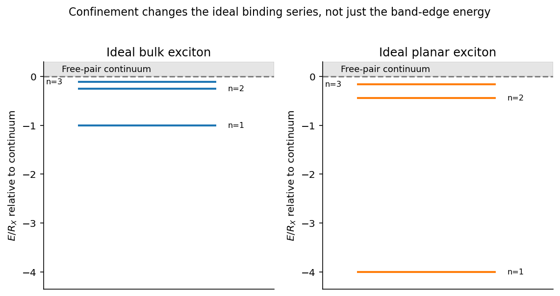
Quantum wells tune both the continuum threshold and the bound-state energy; an optical line shift is not automatically a change in binding alone. The hydrogenic envelope model requires a Wannier-sized state, rather than an exciton localized to one lattice cell.
Start from electrons moving in the periodic equilibrium ionic potential. Displace ion by and expand its contribution as . Quantizing the harmonic normal modes expresses as a sum of creation and annihilation operators with displacement scale for a single simple branch. Expanding the electronic field in bloch states then gives a band-projected Fröhlich HamiltonianHere obey canonical anticommutation relations and remove/create an electron with crystal momentum and spin ; are boson operators for lattice modes. The matrix element contains the derivative of the ionic potential, phonon polarization, displacement normalization and electronic wavefunction overlaps. With phases chosen appropriately, ensures a Hermitian Hamiltonian. The displayed one-band, one-branch notation suppresses additional branch and band labels. “Fröhlich Hamiltonian” here means the linear electron-phonon model used in the question; it is not a requirement to use specifically the polar-optical-phonon coupling of a polar semiconductor. A harmonic lattice, small displacements and a weak enough coupling to organize perturbation theory are the underlying approximations.
The Fröhlich canonical transformation removes real linear phonon operators from the electron-only effective problem to first order. Choose an anti-Hermitian with . For and , one possible generator isIts Hermitian conjugate is its negative after relabelling momenta. The Baker--Campbell--Hausdorff formula givesThe commutator describes virtual emission and absorption of a phonon. normal ordering yields an electron-electron term as well as one-electron energy renormalizations and phonon terms. Retain the former, absorb single-particle shifts into and eliminate the explicit phonon sector. For elastic pair scattering the two virtual time orderings have the combined amplitudeUsing the usual factor one-half to count unordered pairs gives the coefficient in the printed Hamiltonian, with . The two outgoing momenta are and , so total momentum and the spins are conserved. A fully off-shell effective operator can instead use symmetrized denominators for both external legs; the displayed expression is the usual elastic-scattering reduction. Eliminating nearly resonant real phonons requires more care than this second-order construction.
For the denominator is negative: virtual phonon exchange is attractive in this low-energy channel. Physically, an electron changes the ionic density and a second electron can gain energy by responding to the delayed distortion. This is a retarded interaction, not an unscreened instantaneous attraction at every energy transfer. At large transfer the sign changes, and screened Coulomb repulsion must also be included when deciding the net low-energy pairing strength. The connection between lattice dynamics and superconductivity is supported by the isotope effect, but the mathematical attraction alone does not determine a measured transition temperature.[ref]
Electron-Phonon Interactions and Superconductivity by John Bardeen. pp. 55–57, lattice-coupling mechanism and isotope-effect motivation
For the pair calculation, make the model restrictions explicit. The filled Fermi sea is inert, and denotes that sea with no added particles, not an empty electronic vacuum. Project the interaction onto the previously empty shell , where and . Measure the added-pair energy relative to ; this is the negative in the final formula. If absolute one-electron energies are retained in the preceding eigenvalue equation, its eigenvalue must instead be . A shell-restricted state would not in general be an exact eigenstate of the completely unprojected, all-momentum contact Hamiltonian.
Write and . Within the zero-total-momentum pair subspace the two opposite-spin terms cancel the interaction's factor one-half, while same-spin s-wave terms cancel by fermionic antisymmetry. Thus the projected Hamiltonian acts asFor and , matching each basis coefficient givesThis is the stated coefficient formula in the consistent Fermi-level energy convention. Its even dependence on produces an even orbital state with a spin singlet. The constant is fixed up to an overall phase by normalization; for a bound state, . It cannot be set to zero for the nontrivial bound solution.
Put with and impose the sum defining :Here counts orbital states for one spin species, as appropriate to the unrestricted sum in this pair basis, and is approximately constant over the thin shell. If a two-spin total density of states is used, it must be divided by two in this integral. State-counting and the volume convention in and must be consistent. With as the paper's dimensionless coupling, inversion yieldsThe first approximation is the constant-density-of-states, restricted-shell model; the final exponential additionally assumes weak attraction. The binding energy is nonanalytic at zero coupling, so a finite-order power expansion in cannot produce it.
Cooper's problem asks whether two electrons added above an inert Fermi sea bind despite Pauli exclusion of lower states. An arbitrarily weak net attraction binds a zero-momentum singlet below the free-pair threshold, because the near-Fermi-surface integral diverges logarithmically as . Its wavefunction draws on many time-reversed momentum states and becomes dominated by a narrow region near the Fermi surface at weak coupling; the corresponding pair is spatially extended. This establishes a Cooper instability of the unpaired reference state.[ref]
Bound Electron Pairs in a Degenerate Fermi Gas by Leon Neil Cooper. pp. 1189–1190, two added particles above the filled sea and the bound-state criterion
The full superconducting ground state needs a coherent many-electron treatment in which overlapping pairs and the reorganized sea are included. BCS theory supplies that step; the two-electron binding scale alone is neither a calculation of the many-body gap nor a derivation of zero resistance.[ref]Theory of Superconductivity by John Bardeen and others. pp. 1175–1177, paired many-electron ground state and excitation gap
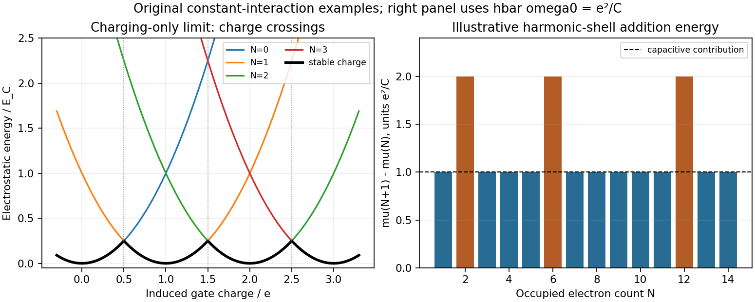
A quantum dot confines electronic motion in all three directions. A semiconductor dot can be thin enough that only one transverse subband is occupied, with discrete lateral states controlled by gates. In a rectangular hard-wall model,A smooth circular lateral confinement is often better approximated by , giving above the transverse ground energy. Shell contains orbitals, twice that many electrons before interactions split the spin degeneracy. Hence closed-shell electron numbers are . These are single-particle quantum numbers; an interacting dot's states are many-electron eigenstates, not simply one orbital occupied by a whole charged island.
A perpendicular magnetic field changes the harmonic spectrum to the Fock-Darwin spectrum. For an electron of charge , take and in the usual symmetric gauge. ThenReversing the definition of the angular label changes the displayed sign of its orbital term, not the set of energies. The Zeeman term lifts spin degeneracy, while exchange can favor parallel-spin filling in partially filled shells. These effects are distinguished by how peaks evolve with field rather than by identifying every irregular peak spacing with one-particle confinement.
For electrostatics, let and , where represents a fixed offset charge in the chosen convention. The constant interaction model givesThe charging energy is conventionally , whereas adjacent charge-state potentials differ byThis addition energy separates a capacitive contribution from orbital spacing. Exchange, nonuniform screening and correlations are corrections to the constant interaction model; a change in dot shape or effective capacitance can also alter spacings.
Connect the island weakly to source and drain reservoirs through tunnel barriers. sequential tunnelling is suppressed in a charge-stable region when neither adding nor removing an electron is energetically accessible. Sweeping the gate brings a charge electrochemical potential through the reservoir Fermi level, giving a Coulomb-blockade conductance peak. The gate lever arm is , so locally if the capacitances and level spectrum do not vary appreciably. At finite source-drain bias, alignment with either reservoir defines the boundaries of a Coulomb diamond. Its slopes constrain capacitance ratios, and lines parallel to its edges can reveal excited-state transport. The conversion from a diamond's bias height to an energy depends on bias convention; a full-height/half-height factor must not be assumed without declaring the circuit.
A clear charging spectrum requires and tunnel broadening smaller than the relevant addition energy; resolving individual orbital levels additionally requires them smaller than the orbital spacing. Tunnel resistances large compared with suppress strong charge fluctuations in the usual weak-junction regime. Blockade is not an assertion of mathematically zero current: higher-order cotunnelling can remain, and strong coupling or low-temperature spin correlations can invalidate the sequential model. An experimental check therefore combines gate sweeps with bias spectroscopy, temperature dependence and barrier tuning to separate level structure from broadening or uncontrolled charge traps.
In a primary vertical-dot experiment, gate-controlled current oscillations were converted into addition energies using finite-bias diamond spectroscopy; varying magnetic field then followed shell and spin filling. Reproducing enhanced addition energies at electron numbers 2 and 6 in several devices strengthened the shell assignment. The electron temperature was independently estimated above the refrigerator base temperature, an essential distinction when judging spectral resolution. Field-dependent reordering also revealed exchange effects beyond a purely spin-degenerate orbital model.[ref]
Shell Filling and Spin Effects in a Few Electron Quantum Dot by S. Tarucha and others. pp. 3613–3616, gate control, finite-bias calibration, sample comparisons, electron-temperature estimate and field-dependent spin filling
Past exam of the chemistry A course of the University of Cambridge 2021 Paper 2 A10 a iii Solution 2026-10-20
Substitutional arsenic has one more valence electron than germanium, so it acts as a donor impurity. Thermal ionization of its shallow bound state supplies mobile conduction-band electrons and leaves fixed positive donor charge. The resulting n-type semiconductor can have even when only a small fraction of host atoms are replaced. Its electrical conductivity then rises because the mobile carrier count increases; the opposite donor charge preserves macroscopic charge neutrality.
This argument assumes that the donors are substantially ionized at the measurement temperature and that the added impurity scattering does not overwhelm the carrier increase. The screened bound-donor picture and its departures from a simple hydrogenic model are described in institutional semiconductor spectroscopy notes.[ref]
Past exam of the chemistry A course of the University of Cambridge 2025 Paper 2 A10 a i Solution 2026-10-20
For an intrinsic, nondegenerate semiconductor, charge neutrality and the Boltzmann approximation to the Fermi-Dirac distribution give . Assume the two polymorphs have equal effective-density-of-states prefactors and retain the quoted band gaps at the temperature being estimated. Their carrier-density ratio is thenwith expressed in eV per kelvin. At ,Both absolute intrinsic densities are extremely small at this temperature; a large ratio does not imply that either material is a good intrinsic conductor. Defects or unintended dopants can dominate real “undoped” specimens.
A band gap is consistent with a semiconductor. In pure gallium phosphide, the valence band is essentially full and the conduction band essentially empty at low temperature; thermal or optical excitation can produce mobile electrons and electron holes.
At room temperature, is much smaller than the band gap, so intrinsic excitation is strongly suppressed. Pure material consequently has a low intrinsic carrier density, while semiconductor doping can markedly increase its electrical conductivity.
Past exam of the condensed matter physics course of the University of Oxford 2021 3 e Solution 2026-10-25
For the degenerate electron gas, let include both spin states. The Sommerfeld expansion givesFor the gapless symmetric intrinsic semiconductor, part (d) gave the same coefficient with . Thus for equal sample areas and equal spin and valley degeneracies,The equality often intended in this comparison requires the same density of states. The source sets but does not explicitly equate them to the electron gas mass . Without that additional assumption the ratio is , or more generally if sample areas or degeneracy factors differ. For example, with equal areas satisfies the stated equal-effective mass condition in the semiconductor and gives ratio two. The filled Fermi sea does not add a factor : only the thermal shell near its Fermi energy contributes to its heat capacity.
Past exam of the condensed matter physics course of the University of Oxford 2022 3 a Solution 2026-10-25
Let , with the Boltzmann constant, the absolute temperature, and the common equilibrium chemical potential. The conduction band minimum and valence band maximum are and ; their separation is the band gap . The positive parameters in the supplied density of states functions are the band effective masses of electrons and electron holes, not necessarily the bare electron mass.
The electron occupation is the Fermi-Dirac distribution . The appropriate statistical factors are for electrons and for electron holes. In a nondegenerate semiconductor, and , so the Boltzmann approximation givesFor the conduction band, set and then . The supplied integral yieldsFor the valence band, set to obtainThe effective density of states factors include the two spin states already present in the supplied density of states functions. Multiplication cancels the chemical potential and gives the semiconductor mass-action lawHere is the intrinsic carrier concentration. Equality additionally requires an electrically neutral intrinsic semiconductor. The product law also applies to an equilibrium doped semiconductor while both populations remain nondegenerate. The derivation assumes parabolic energy bands, the stated spin degeneracy, and a single common chemical potential.
In a conventional superconductor, an attractive pairing interaction forms Cooper pairs and a phase-coherent condensate. The elementary fermionic excitations have a superconducting energy gap ; breaking a pair into two excitations costs at least . The density of thermally excited quasiparticles is exponentially small for . Nevertheless the vanishing DC electrical resistivity below the critical temperature is a property of the coherent supercurrent, not a claim that all thermal quasiparticles disappear. Below the relevant critical-current and critical-field limits, a homogeneous bulk sample carries dissipationless current; above the superconducting transition the normal resistivity returns.
In a semiconductor, the band gap separates filled valence states from empty conduction states because of the periodic crystal potential and orbital hybridization. Thermally exciting carriers across the gap produces both conduction electrons and valence holes. For an intrinsic sample,Thus its electrical resistivity generally rises rapidly on cooling, with an activated factor up to mobility and density-of-states prefactors. This differs from the zero-resistivity condensate response. Dopant freeze-out and extrinsic-carrier regimes require their own activation scales; the intrinsic formula is not universal for every doped sample.
There are two electrons per primitive unit cell; a spin-degenerate energy band accommodates exactly that number. A semiconductor results when the first band is full and does not overlap the second. In the leading two-wave/four-wave approximation, compare the first-band maximum at with the second-band minimum at :This is an indirect band gap; a nonzero local splitting at alone is insufficient. At the onset,With , gives , henceFor more negative than this value the estimated indirect band gap is positive; at equality the bands just touch. This is the onset estimate within the source's nearly-free electron model truncation, not an exact critical potential after coupling all plane waves.
In a direct band gap semiconductor, the small photon momentum makes optical transitions approximately vertical in wave vector. Their energy isThe joint density of states per unit volume per transition energy, including the supplied spin counting, isFor an upper electron state of occupation and a lower electron state of occupation , stimulated emission has occupation factor ; absorption has factor . Their difference is exactly . Multiplication by the joint density of states therefore givesThe proportionality suppresses the optical transition matrix element and other smoothly varying optical prefactors. It assumes parabolic isotropic energy bands, an allowed direct transition, and negligible linewidth and many-body corrections. Here counts electrons, not electron holes.
A quasi-Fermi level is the chemical potential parameter of an approximately thermalized carrier population within one energy band. Rapid intraband scattering can establish a Fermi-Dirac distribution in each energy band before slower interband recombination equilibrates their populations. Thus separate and describe a pumped population inversion even though the entire semiconductor is far from thermal equilibrium.
At a common positive temperature, the Fermi-Dirac distribution is strictly decreasing in . ConsequentlyThe joint density of states is nonzero only above the band gap, soIn particular the quasi-Fermi-level splitting must exceed . The upper boundary is transparency, where stimulated emission balances absorption; the lower boundary has zero joint density of states in this ideal three-dimensional parabolic model. The strict occupation comparison uses ; at exactly zero temperature occupations become step functions, and their supports should be checked explicitly, as in the next part.
Past exam of the mathematics course of the University of Cambridge 2005 ii Paper 4 33B Solution Created 2026-09-24 Updated 2026-10-20
In the nondegenerate regime, lies well inside the gap, with and . Then conduction occupations are approximately , while the hole probability in a valence state is approximately . Using the near-edge density of states and the supplied gamma integral givesThereforeThis assumes the edge approximations are valid over the thermally populated ranges. For an intrinsic semiconductor , so each carrier density is proportional to . Both mobile conduction electrons and holes contribute to conductivity, with mobilities . The exponentially varying carrier densities explain strong temperature dependence even when the mobilities vary only algebraically.
Donors supply electrons and acceptors remove electrons to create holes. With complete ionization and negligible minority carriers, the majority densities are on the n side and on the p side. The corresponding isolated chemical potentials areCarrier diffusion at contact leaves positively charged donors and negatively charged acceptors in a depletion layer. At equilibrium the electrochemical potential is constant; the electron energy shift is . Hence the n-minus-p electric potential isAll quantities must have a consistent normalization: if are state densities per volume, are dopant densities rather than bare atom counts. The formula neglects incomplete ionization, degeneracy and changes in band structure.
At a common temperature the two equilibrium junction/contact effects do not drive a perpetual current. At different junction temperatures, electrons and holes transport entropy differently, giving different Seebeck coefficients on the two sides. The loop has a thermoelectric electromotive force, oriented as , and therefore generally carries current when closed. This is the Seebeck effect: energy is supplied by heat flow from hot to cold. The temperature dependence of the junction barrier is useful intuition, but an exact terminal voltage is not obtained simply by subtracting two equilibrium built-in potentials; it also depends on bulk transport and contact conditions. The given equilibrium density-of-states data do not determine the numerical thermopowers.
Past exam of the mathematics course of the University of Cambridge 2010 ii Paper 3 34B Solution Created 2026-09-24 Updated 2026-10-14
The Bloch theorem says that for a translation-invariant lattice Hamiltonian, eigenstates can be chosen as , or with periodic of period . The localized site orbitals are translates, and . In the tight-binding model, neglect intersite overlap and useProjecting the Schrödinger equation onto each localized orbital gives its onsite energy times its own coefficient, plus the four stated neighbor matrix elements. ThusFor the Bloch amplitudes, set . The coefficient eigenproblem isso the two energy bands areA first Brillouin zone is ; wavevectors differing by are equivalent. Put , . Each band is nonincreasing as a function of , because . HenceThe extrema occur at and at the zone edge; they may be nonunique when , in which case the gap vanishes. In the trial wavefunction, replacing by and reindexing produces exactly the factor , verifying Bloch theorem directly.
An electrical conductor has available nearby unoccupied states in a partially filled band or overlapping bands. A band insulator has filled lower bands separated from empty higher bands by a large gap. A semiconductor has the same filled-band structure with a smaller gap, so thermal excitation or doping supplies mobile electrons and holes. Band filling and carrier availability, not just the existence of two bands, determine which description applies.
One suitable platform is a monolayer molybdenum disulfide semiconductor. An electrostatic accumulation gate supplies conduction electrons whose motion is confined to the atomic sheet; source and drain contacts act as reservoirs. A clean insulating substrate and dielectric or encapsulation reduce disorder and prevent gate leakage. Two split gates deplete the adjacent sheet and leave a narrow conducting gap, thereby confining the in-plane transverse direction while retaining transport along the gap.
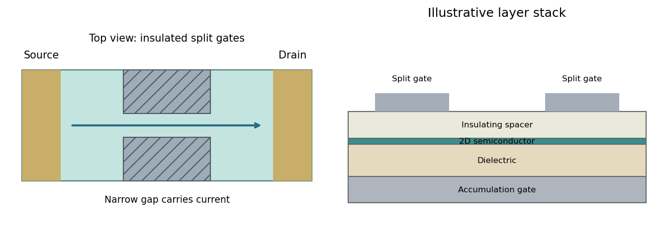


Apply a small source-drain voltage, measure the current and determine linear-response conductance while tuning the split-gate voltage and carrier density. A graphene sheet is another two-dimensional carrier system, but its lack of an ordinary gap complicates purely electrostatic confinement; etched boundaries or a suitable gapped architecture may be needed. A two-dimensional material does not by itself guarantee ballistic transport or resolved subbands.[ref]
Split-gated point-contact in MoS2-hBN structures by Chithra H. Sharma and Madhu Thalakulam. Electrostatic confinement in a two-dimensional semiconductor platform
Relative to conventional crystalline-silicon technology, many organic absorbers offer low-temperature thin-film processing and lightweight flexible devices, but have more strongly bound excitons and more disorder-limited charge transport. These are common material trends, not universal statements about every organic or inorganic device.
Relevant semiconductor properties include the absorption spectrum and optical gap, donor/acceptor energy levels and offsets, dielectric screening and exciton dissociation, electron/hole mobilities, recombination lifetimes, traps and morphological stability. Contacts must extract the appropriate carrier selectively. These properties determine the device quantities inA favourable gap alone does not fix efficiency: current generation, voltage loss and fill factor must all be controlled.
Use Kelvin probe force microscopy to quantify a local contact-potential difference. A conducting tip and sample form a position-dependent capacitor. Apply a voltage with adjustable direct and small alternating components,The electrostatic force is proportional to , so its component at is proportional toup to the chosen force-direction convention. A lock-in amplifier detects this component and a second controller adjusts to null it. At the null, . The compensation voltage becomes the potential image.[ref]
Scanning Probe Microscopy Modes by Bruker. Surface Potential Imaging: conducting probe and electrostatic null measurement
A lift pass can reduce direct topographic interactions. Calibration on a reference with a known work function is required for an absolute work-function interpretation, and the sign convention must state which electrode is biased. On a semiconductor the result can include surface band bending, trapped charge and surface chemistry, so it need not equal a simple map of bulk electrochemical potential.
The measured potential is a spatially weighted electrostatic signal, not an infinitesimal-point voltage. The apex, cone and cantilever all contribute capacitance; increasing lift height weakens the signal and broadens its lateral averaging. Small pits can consequently show reduced or distorted contrast.
Imperfect topographic tracking changes the true separation on the lift pass, producing crosstalk correlated with pit geometry. Tip contamination or work-function drift changes the reference. Adsorbed water, mobile charges, illumination, atmosphere and surface states can change the specimen during measurement; semiconductor band bending can also depend on the applied electrical excitation.
There is a tradeoff between small lift height and suppressing short-range/topographic interference. Repeat at several heights, check trace/retrace and an electrical reference, and compare with independently measured electrical response. A stable potential contrast is evidence of a local electrostatic difference, not by itself proof of a particular dislocation's conductivity.