A diode is a two-terminal component with an asymmetric current-voltage characteristic: reversing its terminal electric potential difference need not reverse its electric current with the same magnitude. Name the terminals diode anode and diode cathode . Define using their electric potentials, and take positive electric current from to . The bar in the diode symbol marks . Positive is the forward direction; negative is the reverse direction.[ref]
The asymmetry makes a rectifier possible: a sinusoid can drive electric current through a resistor on one half of each cycle. An ordinary resistor obeying Ohm's law instead reverses its electric current when the applied electric potential difference reverses. The useful idea is directional selection; the ideal diode model captures it, while the Shockley diode equation describes a smooth exponential function rather than an abrupt switch.
The terminal of a diode at which positive forward electric current enters, with the orientation used in the ideal diode model.
The terminal of a diode at which positive forward electric current leaves. The bar in the diode symbol identifies this terminal.
The ideal diode model sets the conducting electric potential difference to zero and the blocking electric current to zero. With the stated orientation,[ref]
The Junction Diode by W. Marshall Leach, Jr.. The Junction Diode, §1.12.1, printed p. 30: zero forward voltage and zero reverse current idealization
The surrounding electrical circuit chooses the state and remaining value. The two branches meet at . Their product vanishes, so the ideal diode dissipates no power: .
The ideal diode model omits forward drop, reverse leakage, diode reverse breakdown and switching delay.
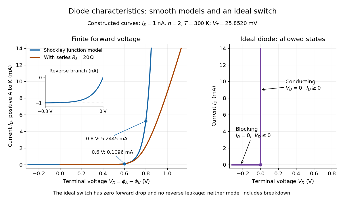
For a p-n junction at fixed temperature, the Shockley diode equation models its electric current asHere is the diode saturation current, the diode ideality factor, the thermal voltage, the Boltzmann constant, and the elementary charge.[ref]
The Junction Diode by W. Marshall Leach, Jr.. The Junction Diode, §1.2, printed p. 4, equation (1.1) and parameter definitions
For an original model example, choose , , and . Using and gives . Then gives , whereas gives . These are predictions of the declared model. There is no universal turn-on electric potential difference: solving the Shockley diode equation for the value needed at a chosen electric current givesAt , increasing by multiplies the electric current by approximately . At the same model gives . Its reverse branch approaches ; it cannot describe diode reverse breakdown.
A constructed extension adds internal series electrical resistance to a junction whose electric potential difference is . Applying the Kirchhoff cycle law givesFor and the same , sustaining needs : across the junction plus across its internal electrical resistance. The derivativeshows why the current-voltage characteristic becomes nearly a straight line when the internal series electrical resistance dominates. This is still a fixed-temperature model; self-heating can change , and . Real diodes also have leakage and charge-storage effects omitted here.[ref]
The Junction Diode by W. Marshall Leach, Jr.. The Junction Diode, §§1.3, 1.8 and 1.11: temperature dependence, charge storage and series bulk resistance
For a long, nondegenerate, ideal p-n junction under low injection, the diode saturation current is set by minority carriers supplied from the neutral regions. Their equilibrium densities are and . Solving the steady diffusion and recombination equations gives , where is junction area, are diffusion coefficients, and are diffusion lengths. Reverse bias suppresses opposite majority-carrier injection exponentially while collecting this minority supply. Thus is approximately bias independent before breakdown, but depends strongly on temperature through and on transport, doping, and geometry.
The positive electric current scale in the Shockley diode equation.
In a diffusion-dominated p-n junction, with a transport prefactor determined by minority-carrier diffusion and dopant densities. Combining this with the intrinsic carrier concentration gives, for fixed gap and effective masses,The slope against is . A measured diode ideality factor helps identify the transport regime: generation or recombination current can have a different dependence on , so its activation slope cannot automatically be interpreted with the diffusion formula.
The dimensionless parameter adjusting the forward slope in the Shockley diode equation. Its ideal junction law sets .
A sufficiently large reverse electric potential difference can produce a rapidly increasing reverse electric current. Both the ideal diode model and the unextended Shockley diode equation omit this behavior.[ref]
The Junction Diode by W. Marshall Leach, Jr.. The Junction Diode, §1.7, printed p. 17: breakdown after the small reverse-current region
The New Jersey Institute of Technology laboratory uses a silicon 1N4148 diode. For its forward current-voltage characteristic, the supply operates in current-source mode; a benchtop voltmeter independently reads the diode electric potential difference. Small electric current steps resolve the steep branch. For reverse measurements, a sensitive ammeter sits in series; the handout suggests a – series resistor. Reversing the applied polarity supplies the comparison. Meter placement must avoid counting the voltmeter's own electric current, and the zero reading may have an offset. The same diode is then measured with an Agilent U2722A source measure unit for graphical comparison.[ref]
Part B Semiconductor Devices: Diodes 1 by New Jersey Institute of Technology. Part B, Experiments with Semiconductor Diodes, items 1 and 2(a): preparation, current control, independent voltage readout, reverse series resistor and same-device comparison
The prescribed analysis uses a logarithmic scale for forward electric current to infer and from the straight region. Large-electric current departures can indicate series electrical resistance. The handout cautions that the accessible range may not determine it precisely; meter loading also matters. This is a measurement procedure, without a published set of device readings.[ref]
Part B Semiconductor Devices: Diodes 1 by New Jersey Institute of Technology. Experiments with Semiconductor Diodes, item 1, parameter extraction and high-current trend-line limitations; Report and Analysis
The reason for the logarithmic scale follows directly from the Shockley diode equation. If and series electrical resistance is negligible,where is a fixed reference electric current making the logarithm dimensionless. The slope is , so extracting needs the junction temperature. Fitting only an appropriate interval matters: a straight-looking subset cannot establish the model at all electric currents.
A rectifier converts an alternating input into a unidirectional output. Diode orientation selects which direction of electric current is transmitted.[ref]
An electrical circuit that uses diodes and capacitors to produce an output electric potential difference larger in magnitude than the input peak. The attainable output depends on the circuit arrangement, electric current drawn by the load, capacitance and input frequency; an ideal unloaded result does not specify the output under load.
For an original ideal example, let an ideal voltage source supply the sinusoid , with and angular frequency . Connect its positive reference terminal to the diode anode, the diode cathode to the upper terminal of a load resistor with electrical resistance , and the lower terminal to the source return. Let be the upper-minus-lower load electric potential difference, and the downward load electric current. Assume the ideal diode model, zero source electrical resistance, and no filter capacitor, inductor or switching delay.
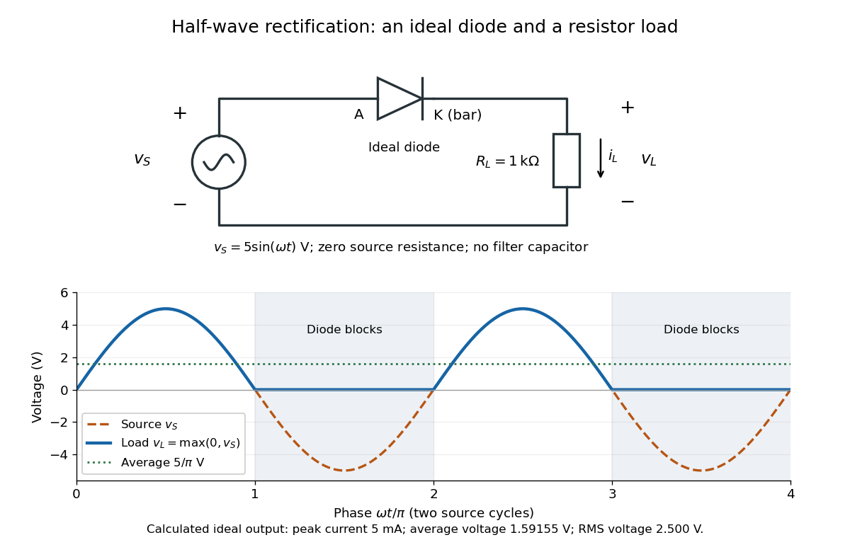
An ideal half-wave rectifier selects the positive half-cycle
. Original schematic and calculated load electric potential difference for and . The diode cathode is the bar at ; positive load electric current flows downward through the resistor. Dashed orange: source sinusoid. Blue: load output, zero during the negative half-cycle. Green: its cycle-average electric potential difference . No smoothing capacitor is present; these are ideal model predictions. Details.The Kirchhoff cycle law gives , and Ohm's law gives . If , the blocking assumption would give , contradicting the ideal diode model, so the diode conducts with . If , conduction would give , also forbidden, so the diode blocks. At the crossings both values vanish. ThusThe peak load electric current is . The output is unidirectional but still varies in time, reaching zero throughout every negative half-cycle. Over a period of a function , write the wave phase as . Its average value of a function and root mean square follow from two integrals:Consequently the average load power is , not . The ideal diode has zero loss; the resistor converts supplied energy into Joule heating. The same switching argument predicts when the diode is reversed. Directional selection changes the waveform and its average value of a function; it does not by itself produce a constant output.
A light-emitting diode is a semiconductor diode producing electroluminescence under electric current. Forward bias injects electrons and electron holes; radiative electron-hole recombination emits photons. A double heterostructure uses band offsets to retain both charge carriers in an active layer. A sufficiently thin layer is a quantum well.[ref]
https://journals.aps.org/rmp/pdf/10.1103/RevModPhys.87.1139. §I, p. 1139, Fig. 1; §IV.A, pp. 1143–1144: injection, active layer and quantum-well distinction
The optical and electrical questions are different: photon energy sets a color scale, while light-emitting diode efficiency determines how much supplied energy escapes as light. The blue light-emitting diode made compact white light-emitting diodes and full-color displays practical. A modulated light-emitting diode can also supply the optical signal in a chopped-light lock-in experiment.
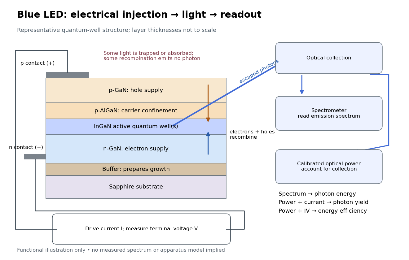
Blue light-emitting diode: carrier injection, emitting structure and optical readout
. Original functional schematic of a representative indium gallium nitride quantum well device on sapphire, not a reconstruction of the 1989 or 1994 devices. Layer thicknesses are schematic. Separate electrical and optical readings determine different properties: terminal electric potential difference and electric current, spectrum, and calibrated escaping optical power. The arrows represent routes through the device rather than a calculated energy band profile. Source. Details.Blue transitions motivate wide-bandgap semiconductors, but a large band gap alone cannot guarantee efficient emission. Gallium nitride has a direct band gap; indium gallium nitride composition tunes the transition energy.[ref]
https://www.kapitza.ras.ru/~glazkov/students/Nobel-akasaki-lecture.pdf. §2, printed pp. 8–10: direct/indirect gaps and nitride composition range
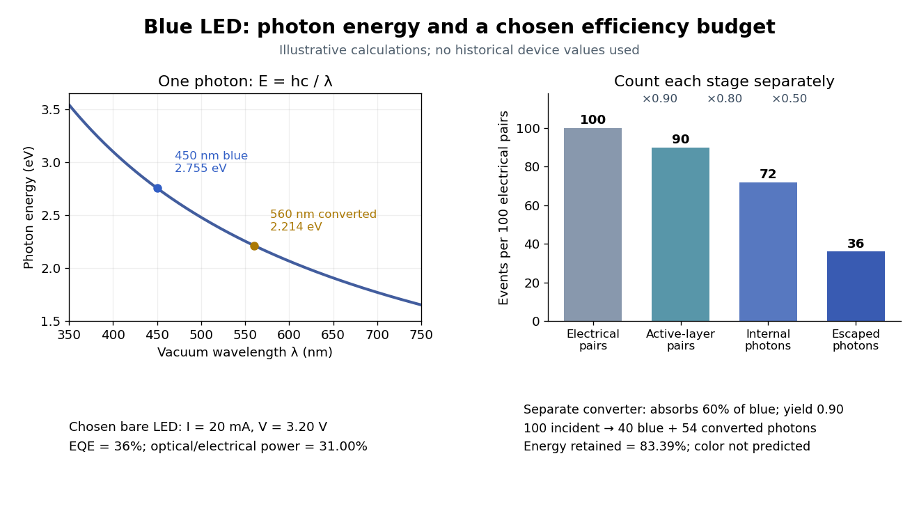
For an emitted photon, with frequency and vacuum wavelength ,where is the Planck constant and the vacuum speed of light. Multiplying energy by wavelength gives . Thus chosen wavelengths and correspond to and : blue requires more energy per photon than red. A stipulated transition energy instead gives , in the ultraviolet. These are conversions, not measured emission lines.
For near-edge emission, estimates the photon energy from the emitting material's band gap. Quantum well confinement or impurity transitions can change it. The 1994 blue light-emitting diode used zinc-doped indium gallium nitride, emitting below its near-edge transition.[ref]
Candela-class high-brightness InGaN⁄AlGaN double-heterostructure blue-light-emitting diodes by Shuji Nakamura and others. p. 1688, Fig. 2 discussion: Zn-related emission
The measured forward terminal electric potential difference is also not fixed by , where is the elementary charge. It depends on electric current, temperature, contacts and series electrical resistance. Even the simple Shockley diode equation with series electrical resistance has , whereas an optical transition does not acquire an extra energy merely because the contact drop increases. Consequently, extracting a band gap from one terminal-voltage reading is not justified.
Isamu Akasaki chose metalorganic vapour-phase epitaxy and sapphire, which tolerated hot Ammonia. Large lattice mismatch hindered film growth. In 1985, Hiroshi Amano and Isamu Akasaki's group developed an aluminium nitride epitaxial buffer layer deposited before hotter gallium nitride growth. The buffer supplies initial growth sites; growing islands join into a continuous film. It improves growth without making the lattices identical. Isamu Akasaki separately credits Shuji Nakamura's 1991 gallium nitride buffer.[ref]
https://www.kapitza.ras.ru/~glazkov/students/Nobel-akasaki-lecture.pdf. §§3.2–4.2, pp. 13–20, Figs. 7–11: growth sequence and microscopy
The 1986 growth paper reports a vertical metalorganic vapour-phase epitaxy reactor, source gases mixed just before delivery to slanted sapphire, and subsequent gallium nitride growth over aluminium nitride. Surface microscopy, X-ray diffraction and photoluminescence tested different aspects of the result. Buffered and unbuffered growth supplied the comparison. Its reported preparation conditions should not be replaced by one universal buffer temperature: the later lecture's account of the first low-temperature trial and the paper's parameter study describe different stages of development.[ref]
Metalorganic vapor phase epitaxial growth of a high quality GaN film using an AlN buffer layer by Hiroshi Amano and others. p. 353, Fig. 1 and Table I; p. 354, surface and diffraction comparisons
A magnesium acceptor impurity in gallium nitride accepts a valence band electron, leaving a mobile electron hole. Hydrogen passivation of magnesium acceptors in gallium nitride suppresses this activity. Post-growth activation restores existing impurities' electrical activity; ionization of active acceptor impurities supplies mobile electron holes. Adding magnesium alone is insufficient.[ref]
In 1989, Hiroshi Amano, Masahiro Kito, Kazumasa Hiramatsu and Isamu Akasaki obtained p-type semiconductor conduction in magnesium-doped gallium nitride using low-energy electron beam irradiation. Hiroshi Amano recalls initially resistive samples, an unreliable hot-probe test, then Masahiro Kito's Hall effect confirmation. A junction irradiated in an M-shaped region emitted in that pattern. Treatment, carrier-sign measurement and spatial emission supplied different evidence. Earlier zinc-doped samples brightened under irradiation without becoming p-type semiconductors: brightness alone did not prove the carrier sign.[ref]
https://journals.aps.org/rmp/pdf/10.1103/RevModPhys.87.1133. §V, pp. 1135–1136, Figs. 3–4; authors of 1989 paper in references, p. 1137
Shuji Nakamura, Takashi Mukai, Masayuki Senoh and Naruhito Iwasa's 1992 thermal-activation paper established another route using annealing in nitrogen. Their companion study compared already conducting films heated in nitrogen with films heated in Ammonia: the latter became highly resistive again. Its hydrogen-complex explanation connected this atmosphere dependence to acceptor impurity passivation. These are thermal treatment and atmosphere comparisons, distinct from the earlier electron beam intervention; neither observation alone images an individual hydrogen complex.[ref]
Thermal Annealing Effects on P-Type Mg-Doped GaN Films by Shuji Nakamura and others. abstract: nitrogen annealing above 700 degrees Celsius and electrical changes
[ref]Hole Compensation Mechanism of P-Type GaN Films by Shuji Nakamura and others. p. 1258, abstract and §§1–2: activation history, nitrogen/ammonia comparison and hydrogenation hypothesis
Shuji Nakamura's two-flow metalorganic chemical vapor deposition reactor, gallium nitride buffer, thermal activation and improved indium gallium nitride growth enabled bright double heterostructure devices, followed by thinner quantum well devices.[ref]
The original 1994 paper by Shuji Nakamura, Takashi Mukai and Masayuki Senoh describes a sapphire/gallium nitride-buffer device with zinc-doped indium gallium nitride emission and aluminium gallium nitride confinement. After nitrogen annealing, etching exposed the n-side for a separate contact. At room temperature, varied forward electric currents gave emission spectra and optical-output curves alongside a current-voltage characteristic. At : output, peak wavelength, terminal electric potential difference. The peak stayed nearly fixed across the current series. The paper omits a complete calibrated collection apparatus; comparisons with earlier devices change several preparation details.[ref]
Candela-class high-brightness InGaN⁄AlGaN double-heterostructure blue-light-emitting diodes by Shuji Nakamura and others. pp. 1687–1688, fabrication and Figs. 1–4
Efficiency has several denominators. Specify a steady electric current , positive terminal electric potential difference , and a simplified narrow emission spectrum with photon energy . Assume at most one radiative photon per injected electron and electron hole pair. Let be the fraction of the electrical pair-supply rate reaching the active layer, the fraction of those pairs recombining radiatively, and the fraction of internally emitted photons that escape. Then counting the successive events givesDefine internal quantum efficiency here conditionally on pairs reaching the active layer: . The internal photon yield per electrical pair is instead . Stating this convention matters when another definition folds injection into internal quantum efficiency. The external quantum efficiency and wall-plug efficiency areThese are photon-count and energy-flow identities for the declared model. For a broad spectrum, replace by the mean escaping photon energy, weighted by photon number, when computing optical power.
A stipulated example chooses , , , , and . For every 100 electrical pairs, 90 reach the active layer, 72 emit internally, and 36 photons escape. Thus , not . Using givesThe dimensional analysis is transparent: , , and . The optical and electrical efficiencies differ because differs from the chosen .
The factors suggest different improvements. Better confinement can reduce injection leakage; suppressing nonradiative recombination raises the radiative fraction; improving light extraction efficiency helps already-emitted photons escape. A photon trapped by total internal reflection has already passed the radiative step and can still be lost through absorption. Improving extraction therefore need not change the internal radiative fraction.
Shuji Nakamura's lecture cautions that why indium gallium nitride emits efficiently despite many defects was not completely settled in that account.[ref]
https://journals.aps.org/rmp/pdf/10.1103/RevModPhys.87.1139. §IV.B, pp. 1144–1145: high defect density, localization hypothesis and stated uncertainty
As an independent consistency check on the 1994 reported values, treating its broad spectrum as monochromatic at the peak givesThis agrees at the quoted precision with the reported . Its optical/electrical power ratio is instead . The first estimate uses a peak in place of a photon-number-weighted mean, so agreement is a consistency check rather than an exact reanalysis of the measured spectrum.
For the convention used in light-emitting diode efficiency, the internally generated photon rate divided by the rate of electron and electron hole pairs reaching the emitting layer. Its denominator must be stated when comparing measurements.
The rate of escaping photons divided by the electrical pair-supply rate in a light-emitting diode. This counts photons rather than comparing optical and electrical power.
The fraction of internally emitted photons that escape a light-emitting diode across the specified optical boundary. Collection by a particular detector adds another factor unless the measurement accounts for all escaping light.
The emitted optical power divided by electrical input power. For the bare-device calculation in light-emitting diode efficiency, ; a complete lamp also consumes power in its driver. Luminous efficacy, measured in lumens per watt, additionally weights the spectrum by human visual sensitivity and is a different quantity.
An additive color display mixes separate red, green and blue emitters. A phosphor-converted white light-emitting diode converts some blue photons to longer-wavelength light in a phosphor, mixing it with unconverted blue to produce perceived white. Hiroshi Amano distinguishes display and phosphor-lighting applications.[ref]
https://journals.aps.org/rmp/pdf/10.1103/RevModPhys.87.1133. §I, p. 1133: full-color displays and phosphor-based white light
To isolate conversion losses, suppose a converter receives 100 blue photons at , absorbs a fraction , and has fluorescence quantum yield : 0.90 converted photons per absorbed blue photon. Stipulate that every converted photon has , that unabsorbed blue is transmitted, and that both outputs escape without further losses. The output is then 40 blue and 54 converted photons. The total photon yield is , while the retained optical energy fraction isThe lower energy of each converted photon matters even if . Combining this stipulated converter with the preceding chosen light-emitting diode gives and an overall optical/electrical power ratio . These chosen narrow lines and photon counts illustrate conversion accounting; they do not establish a white appearance, color quality or luminous efficacy. Those require the full spectrum and a model of human visual sensitivity.
Articles by others on the same topic



Ideally can be thought of as a one-way ticket gate that only lets electrons go in one direction with zero resistance! Real devices do have imperfections however, so there is some resistance.
First they were made out of vacuum tubes, but later semiconductor diodes were invented and became much more widespread.