
Past exam of the quantum condensed matter course of the University of Cambridge 2014 4 Solution 2026-10-18
Nondegenerate carrier product. Assume three-dimensional parabolic energy bands near their extrema, spin degeneracy two, and no additional uncounted valley multiplicity. Near the conduction edge, a Boltzmann approximation to the Fermi-Dirac distribution givesAngular integration and the Gaussian radial integral yieldFor valence electron holes, the empty-state probability is . Measuring electron hole kinetic energy downwards from similarly givesThe factors two count spin once in each band. Multiplying cancels the chemical potential and proves the semiconductor mass-action law:In an intrinsic neutral semiconductor, . In a doped equilibrium semiconductor the same product holds under the stated nondegenerate assumptions, even when . Extra valleys or several valence branches must be included in the effective density-of-states factors rather than counted inconsistently.
Equilibrium junction. Put the p region on the left and the n region on the right. Before contact their majority carriers are electron holes and Electrons, respectively. Diffusion initially sends Electrons from n to p and electron holes from p to n. This leaves negative ionized acceptors on the p side and positive ionized donors on the n side, creating a depletion region and an electric field directed from n to p. At equilibrium this field balances diffusion, so the net electric current vanishes.
For a homojunction the gap remains constant while the conduction band and valence band edges bend downwards from p to n by . The equilibrium chemical potential is flat. Since , the electrostatic potential rises from p to n. The carrier profiles satisfyWith fully ionized nondegenerate dopants, the neutral p side has , , while the neutral n side has , . Thus the Electron concentration rises across the junction and the electron hole concentration falls, with both small relative to the far-side majority densities in much of the depleted region. The ideal depletion approximation neglects these mobile populations when calculating the fixed space electric charge, but the actual equilibrium profiles are smooth.
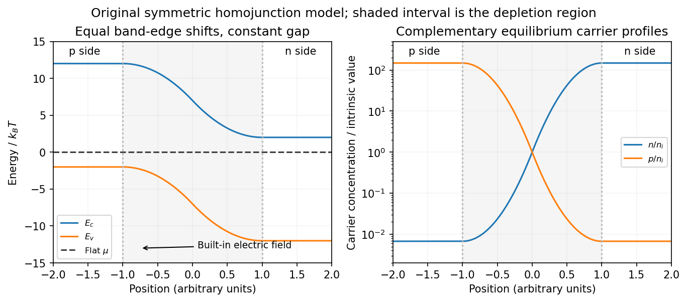
Equilibrium band bending, a flat chemical potential and complementary electron/hole profiles across a homojunction
. Details. The built-in potential follows from these Boltzmann factors:There is no applied terminal bias; the internal electrostatic potential variation does not contradict a constant electrochemical potential.
Opposing carrier fluxes under reverse bias. Use for the magnitude of reverse bias and for reverse electric current, as in the PDF. The junction barrier increases by . The Shockley diode equation in that orientation can be writtenThe reverse-directed contribution is supplied by minority Electrons on the p side and minority electron holes on the n side. They reach the depletion edge by diffusion and are swept across by the built-in field. The opposing contribution is associated with majority carriers thermally crossing the barrier in the forward direction; reverse bias suppresses it by the Boltzmann factor. At zero bias detailed balance makes the two equal, while at large enough reverse bias the opposing flux becomes negligible.
In the ideal neutral-region diffusion model,Here are minority-carrier diffusion coefficients, their diffusion lengths, and is junction area. The two terms inside this positive prefactor are the Electron and electron hole contributions; both flow in the same reverse-current direction. This separates the two carrier-species contributions from the two opposing fluxes in the Shockley diode equation. Calling the saturation term a drift current refers to its passage across the depleted region, and does not eliminate the minority-carrier diffusion needed to supply it.
Reading the measured curves. At , the ideal equation gives , initially proportional to reverse electric potential difference. At , it approaches a plateau . The thermal electric potential differences at the three temperatures are about –, consistent with a rise at small reverse biases and near saturation at larger ones. Higher temperature produces a much larger plateau because thermal electron-hole excitation raises exponentially.
The lower-temperature curve has a noticeable residual electric potential difference dependence rather than a perfectly flat plateau. Depletion-region generation, surface leakage or other departures from the ideal diffusion model can contribute. The sharp upturn at the largest reverse electric potential differences is reverse breakdown, outside the unextended Shockley diode equation; the plot alone does not identify a unique microscopic breakdown mechanism. The original horizontal axis duplicates the final decade label, so a precise breakdown electric potential difference cannot be read reliably. Neither issue prevents estimating the gap from the intermediate-bias saturation region.
Band-gap estimate. Use plateau electric currents at a common intermediate reverse bias, away from both the small-bias rise and the breakdown upturn. Approximate readings are , –, and . Kelvin temperatures are required in the activation law.
For fixed effective masses, . If the remaining transport prefactor is approximately constant, extracting a semiconductor band gap from diode saturation current therefore usesUsing the widest temperature separation and the rounded readings givesNeglecting all algebraic prefactors and fitting instead gives about . These differ by roughly , a material correction on the graph's precision scale. Thus an honest graph-based conclusion isThe nonflat low-temperature plateau, rough electric current readings, unprovided temperature dependence of , and possible gap variation prevent a more precise extraction. If depletion-region generation dominated rather than the specified mechanism, its activation slope could involve a different energy scale; the displayed estimate explicitly uses the diffusion-dominated saturation model requested here.
Past exam of the quantum condensed matter course of the University of Cambridge 2014 3 Solution 2026-10-18
Diagonalization and conventions. The spin-dependent part is . For a Hermitian Hamiltonian is real; the supplied lower-band spinor uses the convention , which will be adopted below. The squared spin matrix is . Hence the two ordered energies areIn the plane, let and . ThenIf , use to retain the energy ordering, and interchange the spin directions assigned below. This is an isotropic Rashba effect; has units of inverse length, whereas has units of energy times length.
Band minima. Define and . Completing the square givesAlong , the radial coordinate is , so the lower branch has two minima:In the full plane these are points on a circle of minima . Both branches meet at , . Their ordered energy curves contain : the lower curve descends from the crossing on either side, while the upper rises. Treating them as globally labeled smooth spin branches without switching labels across would obscure the lower-band minima.
Occupied regions and Fermi contours. At zero temperature each spin-split eigenstate with energy below is occupied. PutFor , . The lower-band roots are and , while the upper band is entirely empty. Thus the central disk is unoccupied, the annulus is singly occupied, and the exterior is unoccupied. Both Fermi circles belong to the lower band; there is no doubly occupied region.
At , the lower band is occupied for , giving a singly occupied disk with outer Fermi circle at . The two bands also meet the Fermi energy at the origin. That isolated degenerate point is not a finite doubly occupied disk, and occupation exactly at the Fermi energy is a boundary convention of zero area. Outside the outer circle the states are empty.
For , . The lower branch has outer radius , while the upper branch has inner radius . The disk is doubly occupied, with one state in each band at every momentum. The annulus is singly occupied, in the lower band only, and the exterior is unoccupied. These are the Fermi contours of an isotropic Rashba band; double occupancy here refers to two orthogonal spinor states at the same momentum, not two Electrons occupying one identical quantum state.
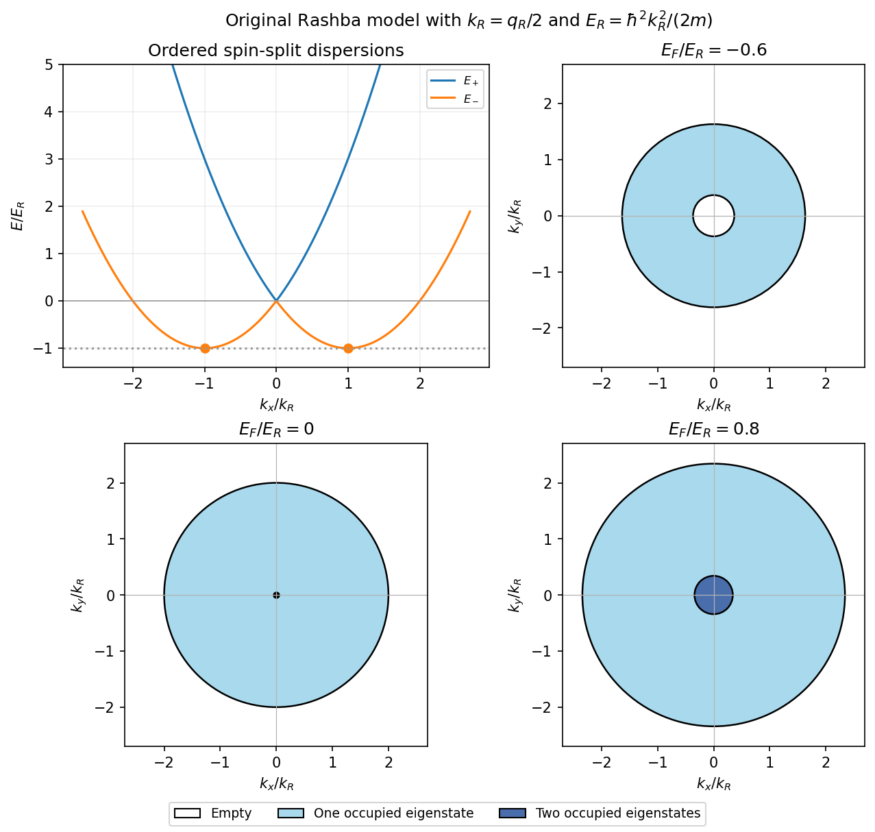
Rashba dispersion and occupied momentum regions below, at and above the band crossing
. Details. Inferring the splitting. Above the crossing, the two positive radii differ by :The minimum radius is therefore . It is the difference of the measured radii that is required for ; below the crossing the two lower-band radii instead add to .
Spinors and spin direction. Write , which has for . An orthogonal normalized partner to the supplied lower-band state isIndeed . Direct multiplication by the spin matrix gives eigenvalues and for and , respectively, so orthogonality has selected the other band rather than merely another arbitrary spin basis.
For a normalized spinor , the Pauli expectation values are . Consequently the Rashba spin texture isThe spin lies in the plane and is perpendicular to momentum. On the outer circle , which belongs to , it points clockwise as viewed from ; at it points along . On the inner circle , belonging to , it points counterclockwise; at it points along . Opposite momenta have opposite spins, consistent with time-reversal symmetry. At the origin the eigenstates are degenerate and no unique spin orientation is defined.
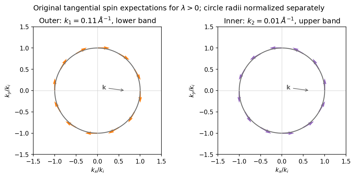
Opposite tangential spin textures on the outer lower-band and inner upper-band Fermi circles
. Details. Past exam of the quantum condensed matter course of the University of Cambridge 2013 4 Solution 2026-10-18
Why degenerate perturbation theory is needed. If several unperturbed states have equal or nearly equal energy, a perturbation can mix them at leading order. In that subspace, diagonalize the perturbation matrix rather than using nondegenerate formulas with small energy denominators. The resulting eigenvectors identify the combinations selected by the coupling, and the eigenvalues give the leading splitting. Other remote states can then be included perturbatively.
For the linear combination of atomic orbitals description of molecular hydrogen, equivalent atomic states on the two nuclei supply the nearly degenerate starting functions. In an orthonormal two-state model, equal diagonal energy and real hopping give and symmetric/antisymmetric combinations. For actual overlapping atomic functions with overlap and Hamiltonian coupling , one instead solves a generalized eigenvalue problem:The bonding state has enhanced density between the nuclei and the antibonding state a separating node. Two opposite-spin Electrons occupying the bonding molecular orbital describe the simplest closed-shell hydrogen-molecule bond. Electron-electron interaction and nuclear repulsion are needed to calculate a realistic total binding energy; the two-state splitting alone is not the full molecular energy.
In the nearly-free electron model, the analogous degenerate states are plane waves and at a Bragg scattering. A Fourier coefficient of the periodic potential couples them. At exact degeneracy , diagonalizing their two-by-two matrix givesThe associated standing waves place electronic density differently relative to the ionic potential. These are the same gap-opening combinations illustrated in Q1(b). The labels of the two starting basis states survive as mixed orbital or plane-wave character, rather than independent crossing eigenstates.
Origin of broad and narrow bands. Spatially extended s/p-derived orbitals have substantial overlap and therefore large hopping amplitudes and broad bands. More localized d orbitals overlap less strongly and produce narrower bands. A multiorbital tight-binding calculation assigns the on-site orbital energies and hopping matrices, forms Bloch sums, and diagonalizes the resulting matrix at each wavevector. Different hopping ranges and orbital symmetry determine the bandwidths and allowed interband coupling. The two-band description retains one broad combination and one nearly flat d-derived combination; a real transition metal contains several d orbitals and more complicated dispersions.
Hybridized eigenvalues and eigenstates. Let , in an orthonormal basis. Hermitian operator fixes the reverse coupling to be . Projection onto the two components givesSolving this quadratic yields the band hybridization dispersionFor nonzero , one eigenvector representation is , followed by normalization. Thus the wavefunctions exchange broad-band and d-band character through the avoided crossing; the levels are equal mixtures at the uncoupled crossing.
At , the parabola crosses the horizontal level at , with . For small nonzero , the curves avoid crossing with minimum direct separation . The lower branch follows the parabola below the crossing and flattens toward above it; the upper does the opposite. The lower branch satisfies everywhere and tends to from below as , while the upper branch always lies above . This is the perfectly flat-band continuum approximation, with zone-boundary intersections excluded as requested.
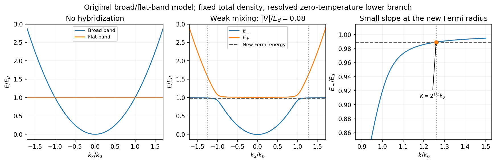
Uncoupled and weakly hybridized broad/flat bands, with the shifted Fermi radius and small lower-band slope
. Details. Fixed particle number and the larger Fermi sphere. Denote the uncoupled broad-band Fermi radius by to distinguish it from the new one . With two spin states, the broad-band number density at is . The stipulated equal population in the flat sector makes the total density twice that value. At zero temperature and any nonzero hybridization, all occupied states fit into the monotonic lower branch below , while the upper branch is empty. ThereforeThis is the stated factor increase. It uses fixed total particle number, equal spin counting, an exactly flat unhybridized band and enough available states below any Brillouin-zone restriction. In generic pairs of dispersive bands both hybridized pockets can remain occupied; then Fermi-volume conservation in two hybridized electron bands fixes a sum of volumes rather than this one radius. The exactly flat band is degenerate at , so its initial occupation must be specified, as it is here.
Fermi-velocity suppression. Set . The exact derivative of the lower branch isAt , and . For , the square bracket divided by two is . Since group velocity is and the broad-band reference velocity is ,so the flat-band hybridization Fermi-velocity suppression isThe reference velocity is that of the original broad-band Fermi sphere, not the broad-band slope at the larger ; omitting the radius change loses the factor .
The low-temperature qualification becomes more stringent as : the new chemical potential approaches with , and the relevant thermal energy must be small compared with this hybridization scale. At fixed nonzero temperature the singular flat-band redistribution is not automatically resolved for arbitrarily small coupling. A small but finite narrow-band dispersion can also change the occupation topology.
Density of states and magnetism. For an isotropic three-dimensional branch with spin degeneracy two,A small Fermi velocity therefore produces a large density of states. The localized, partially filled d-derived bands in iron, cobalt and nickel place many states close to the Fermi level; broad s/p-derived conduction bands in copper, silver and gold coexist with filled d bands lying below it. This explains the substantially larger Fermi-level density of states of the former group within the band picture. An exact factor of ten requires the actual band parameters and is not fixed by the two-band toy model.
A high density of states lowers the kinetic-energy cost of spin polarization. A repulsive exchange interaction can then satisfy the Stoner criterion and stabilize ferromagnetism. With a single-spin density of states and an on-site interaction normalization, the criterion is ; with spin-summed , it is . The large d-state contribution favors this instability in Fe, Co and Ni. The noble metals do not satisfy the corresponding instability condition in the same ordinary state; this does not imply that they have no weak magnetic response whatsoever.
Past exam of the quantum condensed matter course of the University of Cambridge 2013 3 Solution 2026-10-18
Dopant atoms and carrier type. Substitutional semiconductor doping places a small fraction of foreign atoms on host lattice sites. In a tetrahedrally bonded group-IV semiconductor, a group-V substitution such as phosphorus in silicon has an extra valence Electron. A shallow donor level just below the conduction edge can release that Electron, leaving a positively charged donor. In an n-type semiconductor, mobile Electrons are the majority carriers and the chemical potential shifts toward the conduction band.
A group-III substitution such as boron in silicon has one fewer valence Electron. An acceptor level just above the valence edge captures an Electron from the valence states, leaving a mobile electron hole and a negatively charged acceptor. In a p-type semiconductor, electron holes are the majority carriers and the chemical potential shifts toward the valence band. The material can remain electrically neutral in both cases: mobile carrier electric charge is compensated by fixed ionized impurity electric charge. Dopant freeze-out, compensation and degeneracy qualify the simplest one-carrier-per-dopant picture.
Making the junction. Choose p material at and n material at . Electrons initially diffuse from n to p, and electron holes from p to n, recombining near the interface. Negative ionized acceptors are exposed on the p side and positive ionized donors on the n side. They produce an electric field directed from n to p. The field opposes further majority-carrier diffusion until drift and diffusion balance and the equilibrium electrochemical potential is uniform.
The depletion regions are depleted of mobile majority carriers, not of the fixed dopant charges that create the space charge. At equilibrium the conduction and valence edges bend together, while the chemical potential is flat. The specified is a electric potential difference: the corresponding initial chemical-potential energy separation is . This convention is required by the quoted units and width formulas. Write for the absolute permittivity; the paper's is relative permittivity.
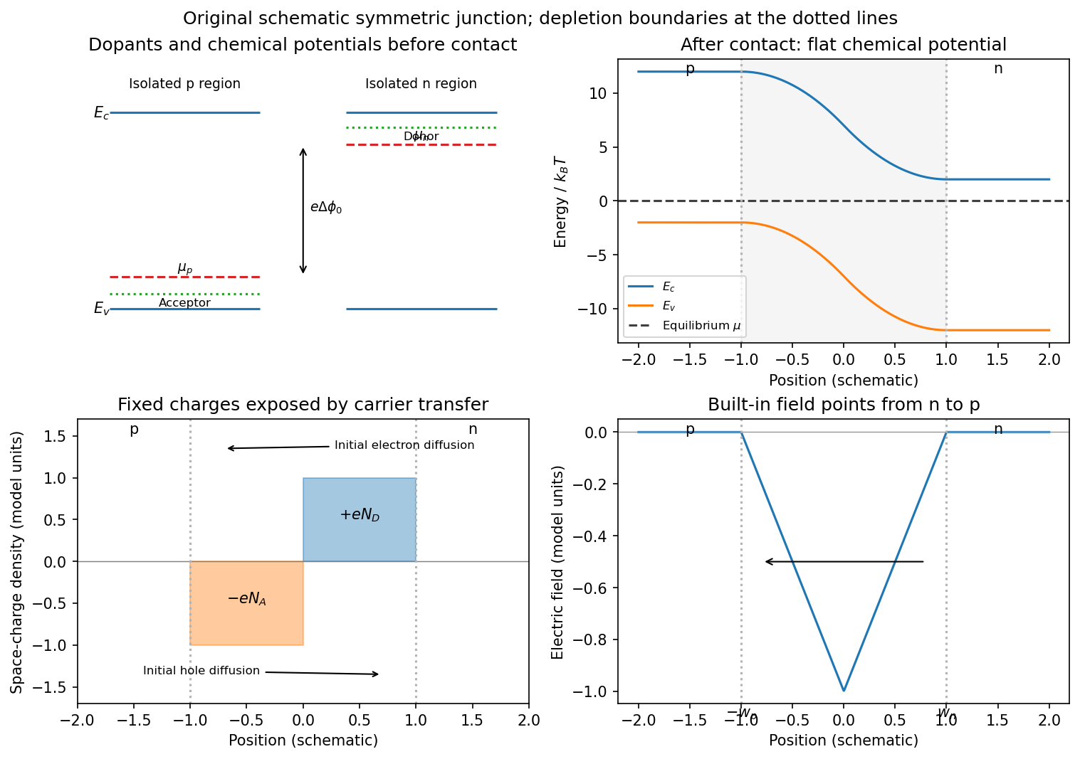
Substitutional donor/acceptor levels, equilibrium band bending, fixed space charge and the junction electric field
. Details. Poisson equation and widths. Let the depleted intervals be and . Fully ionized number densities correspond to electric charge densities , respectively. ThusThe factor converts a dopant concentration to a space-charge density. Requiring zero field in both neutral regions gives charge neutrality,With , direct integration gives the triangular fieldContinuity at the interface is the same neutrality condition. The field is negative throughout the depleted interval. Set . Its integral givesPotential continuity therefore requiresCombining it with neutrality yields the abrupt-junction depletion width and capacitance resultsThe more lightly doped side depletes farther, because equal and opposite space charges must be exposed.
Applied bias. Define positive as forward bias, raising the p-side terminal potential relative to the n-side terminal. It lowers the remaining barrier from to . Reverse bias has and raises that barrier. The same Poisson integration applies, with this replacement:Forward bias narrows the depleted region; reverse bias widens it. Under bias there need not be one equilibrium chemical potential across the device, so the equilibrium flat-level argument must not be reapplied unchanged. The barrier/width change is illustrated in the next figure.
Differential capacitance and electric charge sign. Put and . The signed p-side fixed electric charge per unit area isDifferentiating with respect to forward electric potential difference gives the positive capacitance per unit areaThe n-side electric charge is , so instead. If denotes a positive space-charge magnitude, the positive capacitance is for this forward-voltage convention. This resolves the sign implicit in the paper's positive . The total device capacitance is , where is its cross-sectional area.
Finite device and numerical sketch. For the symmetric device, and each side has thickness . Before full depletion,Using , the zero-bias width on each side is , less than . The total zero-bias capacitance is .
Full depletion occurs when , soAt larger reverse bias the depleted thickness cannot exceed . In the ideal fully depleted slab, incremental terminal electric charge changes the field uniformly through that fixed thickness, giving the full-depletion capacitance of a symmetric junction slabThus the idealized piecewise sketch over the specified range isIt is continuous at full depletion, rises through at zero bias, and has a formal inverse-square-root divergence as from below.
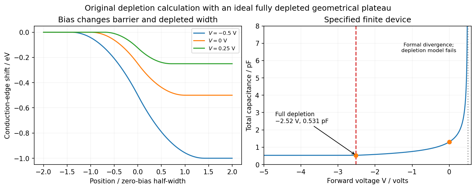


There are two physical limits to this extension. Once all dopants are exposed, their fixed space charge no longer increases, but the terminal electrodes can still acquire incremental electric charge; differentiating only the fixed ionized electric charge would incorrectly predict zero capacitance. Near , the depletion approximation itself fails as mobile carriers and forward injection become important, so the formal infinite endpoint is not a prediction of an actual infinite measured capacitance. The fully depleted plateau assumes ideal contacts and no breakdown, injection storage or extra series capacitance.
There are unlisted articles, also show them or only show them.