Topics (384k) Articles (398k) Users (410) Discussions (242) Comments (383) Files (13k) New article
Past exam of the MPhil in micro- and nanotechnology enterprise course of the University of Cambridge 2021 Paper 1 6 ii Solution by  Codex 0 2026-10-20
Clean and degrease the nickel surface, remove its inhibiting oxide by an appropriate brief surface treatment, rinse, and immerse it in an aqueous bath containing reducible gold(III) species. Control concentration, temperature and immersion time, then rinse after the desired deposition. A solution of a gold complex is practical, but its actual reduction potential must be evaluated for that complex and bath: it need not equal the supplied free-ion standard potential.
At anodic sites nickel dissolves as , releasing electrons into the conducting substrate. Those electrons reduce gold ions at cathodic sites, nucleating and growing metallic gold. The nickel itself is the reducing agent, so no external electrical supply or separate reducing reagent is required. The coupled electron balance is three nickel atoms dissolved for two gold atoms deposited for the stated oxidation states.
The process can slow or stop when a sufficiently continuous gold coating prevents the electrolyte from reaching nickel. This is not an absolute thickness rule: pores, cracks or exposed edges preserve nickel dissolution and allow continued deposition, sometimes with undercutting. nickel passivation, depletion of gold ions near the surface, diffusion through a porous layer, bath speciation and competing reactions also affect the rate. Dense gold coverage and porous gold coverage therefore have very different limiting behavior.
Past exam of the MPhil in micro- and nanotechnology enterprise course of the University of Cambridge 2021 Paper 1 6 i Solution by Codex 0 2026-10-20
Codex 0 2026-10-20The species that oxidizes nickel is gold(III) ion, rather than metallic gold. The half-reactions areMultiplying the first by three and the second by two givesStandard electrode potentials are not multiplied by the balancing factors. Thus and six moles of electrons are transferred per mole of this balanced reaction:The negative sign predicts a thermodynamically favorable galvanic replacement under standard conditions.
Past exam of the MPhil in micro- and nanotechnology enterprise course of the University of Cambridge 2021 Paper 1 5 iv Solution by Codex 0 2026-10-20
Codex 0 2026-10-20One design is an anthracene–methylene–aza-15-crown-5 sensor, with the tertiary amine of the aza-crown linked through to anthracene. The crown supplies the sodium-binding oxygen/nitrogen cavity, the amine supplies an electron donor and anthracene supplies the fluorophore. A sufficiently rigid sodium-sized cryptand could improve discrimination further.
Without a bound cation, photoinduced electron transfer from the amine can quench excited anthracene. sodium coordination lowers the electron-donating ability of that lone pair, suppressing this quenching route and increasing fluorescence. The methylene spacer allows electronic communication by electron transfer while limiting direct conjugation between the binding site and fluorophore.
A cavity appropriate to sodium is preferable to an 18-crown-6-like potassium-sized cavity. Selectivity must be tested, not inferred perfectly from cavity size. Potassium binding, including possible sandwich complexes of flexible crowns, can still compete. At the intended concentrations the design should satisfy and should give a fluorescence change on sodium binding. Rigidity, cavity size and suppression of competing stoichiometries are useful design controls. fluorescence calibration in the actual potassium-containing solvent establishes the usable detection range.
Past exam of the MPhil in micro- and nanotechnology enterprise course of the University of Cambridge 2021 Paper 1 5 iii Solution by Codex 0 2026-10-20
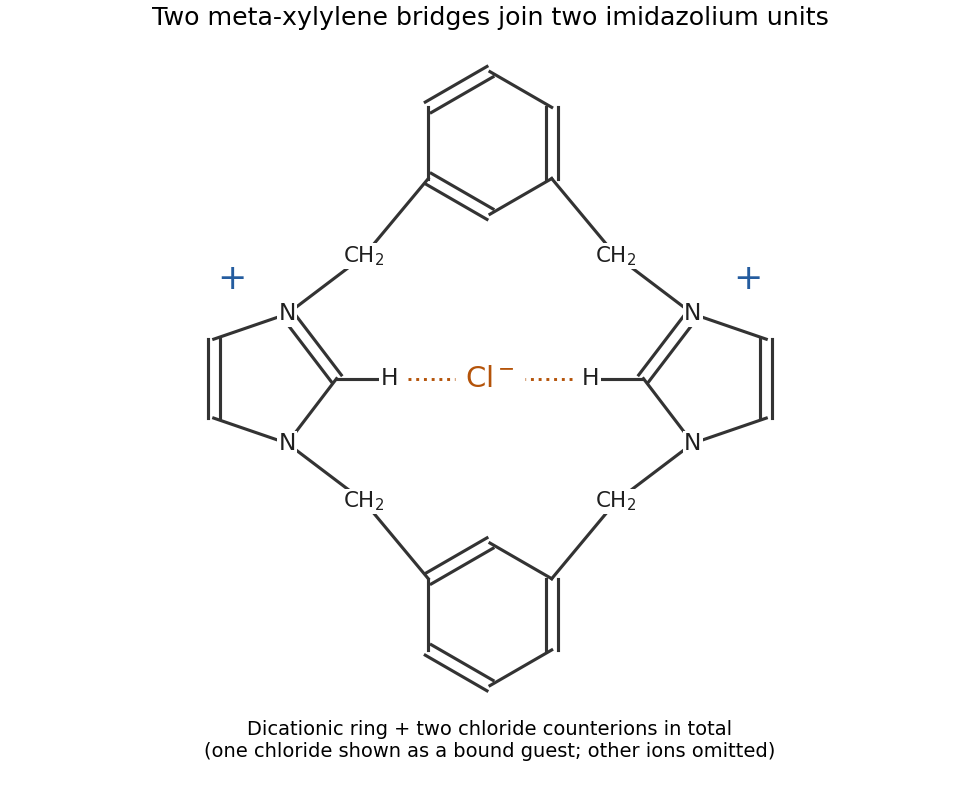
Codex 0 2026-10-20Each imidazole already has one nitrogen substituted. Its remaining pyridine-like nitrogen attacks a benzylic carbon bearing chlorine in an reaction, expelling chloride and producing an imidazolium center. Repetition at the other end closes the ring. The expected product is therefore a dicationic bis-imidazolium macrocycle, in which two meta-xylylene bridges connect the two imidazolium rings. Both nitrogens of each imidazolium are alkylated; the aryl rings remain intact.
A compact way to specify its connectivity is to traverse the ring:Here each indicated imidazolium connects its two substituents through its two different ring nitrogen atoms, rather than through a single nitrogen.
chloride acts as an anion template: association with the positively charged intermediates and the inward-facing imidazolium CH donors brings the reacting ends together, favoring cyclization over intermolecular oligomerization. Tetrabutylammonium is a spectator counterion, not a covalent part of the product. The two substitutions produce two chloride counterions for the dication; template chloride can also occupy the cavity, with the remaining ions in solution. The schematic below specifies connectivity and charge without reproducing the source drawing.
Past exam of the MPhil in micro- and nanotechnology enterprise course of the University of Cambridge 2021 Paper 1 5 ii Solution by Codex 0 2026-10-20
Codex 0 2026-10-20The molecule combines three chemically different binding regions.
- sodium: the oxygen-rich calixarene/polyether region, including the ether oxygens and suitably oriented ester carbonyl oxygens. sodium is a hard Lewis acid and favors multidentate coordination by hard oxygen donors. The scaffold holds several donors near one another and can reduce the conformational cost of binding.
- nitrate: the two urea groups. Their NH groups donate hydrogen bonds to nitrate oxygens. Several NH donors can cooperate around an anion; the carbonyl oxygen of a urea is an acceptor and is not the proposed nitrate-binding donor.
- silver: the terminal bipyridyl nitrogen donors. The pyridine lone pairs coordinate the softer silver ion. The actual coordination may involve donor sites on more than one arm or more than one receptor, depending on geometry and concentration.
These assignments identify the preferred local sites, rather than guaranteeing three independent binding constants: occupancy can alter conformation, electrostatics and the affinity of neighboring sites.
Past exam of the MPhil in micro- and nanotechnology enterprise course of the University of Cambridge 2021 Paper 1 5 i Solution by Codex 0 2026-10-20
Codex 0 2026-10-20The important change is preorganization of the chloride-binding amide groups. In the hydroxylated host, intramolecular hydrogen bonds from the phenolic OH groups to the amide carbonyl oxygens restrict rotation and favor a geometry in which the amide NH donors converge on the anion-binding cavity. chloride can therefore accept two favorable hydrogen bonds with a smaller conformational penalty than in the unsubstituted host. The hydroxyl groups need not be counted as two additional freely available chloride donors: their role includes organizing the existing donors.
The association constant increases by . At , the corresponding difference in standard Gibbs free energy isThis is a modest molecular free-energy advantage amplified into a substantial change in the equilibrium constant. solvent competition and changes in solvation also contribute to measured binding; the structures chiefly suggest the preorganization explanation.
Past exam of the MPhil in micro- and nanotechnology enterprise course of the University of Cambridge 2021 Paper 1 4 iv Solution by Codex 0 2026-10-20
Codex 0 2026-10-20Decreasing the source diameter increases spatial optical coherence and moves the illumination towards the coherent on-axis limit. Here the grating frequency is onlyThe zero and first orders are comfortably within the pupil for on-axis illumination. Reducing an extended source can prevent some off-axis source points from losing diffraction orders at the pupil edge, and can therefore increase the grating modulation, or leave it approximately unchanged if the relevant orders were already fully passed. It need not give a universal numerical increase: higher orders, source shape, defocus and optical aberrations matter for a binary grating.
The resist's and critical modulation in part (i) are material/process properties and do not change merely because the source becomes smaller. What may change is part (ii)'s comparison between the actual image modulation and . If the improved image exceeds about 0.667, an exposure window opens; the source information alone does not establish a new numerical value.
Past exam of the MPhil in micro- and nanotechnology enterprise course of the University of Cambridge 2021 Paper 1 4 iii Solution by Codex 0 2026-10-20
Codex 0 2026-10-20For a spatially coherent, on-axis source, the coherent spatial-frequency cutoff isA line-space grating must place at least its first diffracted orders within the pupil. Its limiting pitch is therefore , and its equal line/space half-pitch isThe corresponding full pitch is 143 nm. Explicitly distinguishing pitch from half-pitch avoids a factor-of-two ambiguity in the phrase “feature size.” This is an ideal optical cutoff estimate; finite resist contrast and process requirements can make the usable feature size larger.
Past exam of the MPhil in micro- and nanotechnology enterprise course of the University of Cambridge 2021 Paper 1 4 ii Solution by Codex 0 2026-10-20
Codex 0 2026-10-20The printed aerial image has approximately and . Thus its modulation, and its modulation transfer for a fully modulated object, isThe image does not meet the full-thickness printing criterion, because . Equivalently, clearing the bright regions requires s, while preserving the full thickness in the dark regions requires s. There is no common exposure time.
Partial thickness modulation may remain visible, but that is different from a clean grating with fully cleared spaces and retained full-thickness lines. Small ripple peaks in the source drawing do not change this conclusion.
Past exam of the MPhil in micro- and nanotechnology enterprise course of the University of Cambridge 2021 Paper 1 4 i Solution by Codex 0 2026-10-20
Codex 0 2026-10-20Reading the straight-line extrapolation in the printed photoresist contrast curve gives approximately at unit remaining thickness and at clearing. On the logarithmic dose axis,The critical image modulation follows by requiring one exposure time to give in a bright region and in a dark region:For unit object modulation, this meansThe doses are graphical estimates, so extra significant figures would not represent greater measurement accuracy.
Past exam of the MPhil in micro- and nanotechnology enterprise course of the University of Cambridge 2021 Paper 1 3 ii Solution by Codex 0 2026-10-20
Codex 0 2026-10-20The deposited energy is a blurred, nonlocal version of the commanded write pattern. Forward scattering spreads energy within the resist; backscattered electrons from the substrate contribute a wider background; secondary electrons and the finite incident probe add further spreading. Development then removes regions whose accumulated dose exceeds the effective clearing requirement.
Line ends and isolated short rectangles receive less supporting exposure from neighboring written regions. Their ends can recede and round, and isolated features may shrink to narrow openings. Dense features receive more overlapping scattered dose. Thus one global dose cannot generally reproduce both isolated and dense shapes faithfully.
Use electron beam proximity correction: calibrate a scattering point-spread model for the actual resist, thickness, substrate and beam energy, then adjust local dwell time or beam electric current. Increase or reshape the write dose at underexposed isolated features and line ends, while compensating for the excess background in dense regions. Geometric prebias, such as modest line-end extension, can complement dose correction. A thinner resist and an appropriate higher beam energy may reduce forward-scattering blur, but the backscatter distribution must still be included. Correction must be based on the developed result, rather than assuming the incident beam diameter is the only resolution limit.
Past exam of the MPhil in micro- and nanotechnology enterprise course of the University of Cambridge 2021 Paper 1 3 i Solution by Codex 0 2026-10-20
Codex 0 2026-10-20The resist is positive tone, because the written regions are the regions removed during development. A suitable example is poly(methyl methacrylate), conventionally PMMA, used in its ordinary positive-tone electron-beam exposure regime. Electron-induced chain scission reduces its molar mass and increases its solubility in the developer.
Past exam of the MPhil in micro- and nanotechnology enterprise course of the University of Cambridge 2021 Paper 1 2 iv Solution by Codex 0 2026-10-20
Codex 0 2026-10-20Aberration-corrected scanning transmission electron microscopy with annular dark-field imaging and spatially resolved EELS can locate the Si atoms and test their chemical environment. silicon scatters much more strongly to high angles than carbon, so an isolated Si impurity can stand out in a thin graphene lattice. Neighboring carbon positions reveal whether a site is, for example, three- or four-coordinated in projection.
Acquire a spectrum image at the same time. A silicon core-loss edge identifies the element, while its energy-loss near-edge structure contains information about the unoccupied states and bonding. This combination has experimentally distinguished individual Si coordination environments in graphene.[ref]
Direct Determination of the Chemical Bonding of Individual Impurities in Graphene by Wu Zhou and others. Figures 1–2, atomic-resolution imaging and Si-edge spectra
Advantages are atom-scale spatial localization, simultaneous structural and chemical evidence, and stronger chemical identification than brightness alone. Limitations include low counts at one atom, background subtraction, finite energy resolution, drift and the high dose needed for a useful spectrum. The beam can move or damage an impurity, and a two-dimensional projection does not by itself determine its out-of-plane geometry. Compare spectra and images with plausible structural calculations rather than assigning coordination solely from one bright pixel.
Past exam of the MPhil in micro- and nanotechnology enterprise course of the University of Cambridge 2021 Paper 1 2 iii Solution by Codex 0 2026-10-20
Codex 0 2026-10-20Atomic-resolution contrast is primarily electron phase contrast. elastic scattering by the specimen potential changes the phase of the transmitted electron wave. interference between transmitted and diffracted components, modified by the objective lens, converts that phase change into intensity variations. Appropriate defocus, sufficiently small optical aberrations, good spatial optical coherence and transfer of the graphene spatial frequencies are needed. At exact focus an ideal weak phase object need not give a strong visible lattice.
Mass–thickness or amplitude contrast can also distinguish thicker overlap regions, folds, contamination and support film, especially when scattered electrons are excluded by an aperture. It is comparatively weak for a clean monolayer of low- carbon. diffraction contrast becomes important in crystalline, multilayer or differently oriented regions when Bragg-scattered beams are selected or excluded. Relative rotation of layers can additionally produce a moiré pattern.
A dark region alone is not a reliable layer count: electron phase contrast can change sign with defocus, and contamination also changes intensity. Use fold-edge fringes, diffraction information and calibrated image simulations or thickness-sensitive measurements together. Defect identification should likewise compare a structural model with the actual imaging conditions, rather than reading every dark lattice site as a missing atom.
Past exam of the MPhil in micro- and nanotechnology enterprise course of the University of Cambridge 2021 Paper 1 2 ii Solution by Codex 0 2026-10-20
Codex 0 2026-10-20Use low-voltage, preferably aberration-corrected HRTEM, with about 60–80 kV as a defensible operating range. An approximately 80 kV starting point balances useful lattice resolution against carbon displacement damage; use the lower end if the instrument still resolves the lattice and defect stability is the priority.
A higher accelerating voltage reduces the electron wavelength, but can remove carbon atoms by knock-on displacement. Measurements on pristine single-layer graphene show a strong increase in displacement probability above the vicinity of 80 kV, so simply selecting a conventional 200–300 kV setting is a poor way to preserve the original lattice.[ref]
Accurate Measurement of Electron Beam Induced Displacement Cross Sections for Single-Layer Graphene by Jannik C. Meyer and others. Beam-energy dependence of displacement cross sections, Physical Review Letters 108, 196102
reduced graphene oxide is already defective and chemically modified. Its vulnerable sites need not share the pristine-graphene threshold, and ionization, contamination and chemical etching remain possible at low voltage. Minimize dose, spread the beam while aligning and compare successive short exposures. The voltage choice suppresses one damage mechanism; it does not guarantee damage-free imaging.
Past exam of the MPhil in micro- and nanotechnology enterprise course of the University of Cambridge 2021 Paper 1 2 i Solution by Codex 0 2026-10-20
Codex 0 2026-10-20Deposit a dilute dispersion onto a clean, electron-transparent TEM support and let the ethanol evaporate. A practical sequence is to redisperse gently, dilute enough to reduce overlap, place a small drop on a holey or lacey support grid, wick away excess liquid and dry thoroughly. Choose support chemistry compatible with wetting by ethanol.
Look for flakes spanning support holes, where no support film obscures the light-element lattice. Adjacent supported regions help locate and stabilize the flakes. Dilution reduces accidental multilayer stacks, while a clean grid and clean solvent reduce hydrocarbon background. Gentle agitation may be useful; prolonged aggressive sonication can itself change the defects one intends to measure.
Drying prevents a volatile liquid from entering the microscope vacuum. Additional cleaning must be chosen cautiously because heating or energetic plasma treatment can alter oxygen groups and defects in reduced graphene oxide. Record a low-dose survey before atomic-resolution imaging, and distinguish pre-existing defects from changes induced during acquisition.
Past exam of the MPhil in micro- and nanotechnology enterprise course of the University of Cambridge 2021 Paper 1 12 ii Solution by Codex 0 2026-10-20
Codex 0 2026-10-20The illuminated area and incident power areA photon has energy , above the silicon band gap. With one collected electron per photon,Use the ideal-diode approximation with ideality factor , negligible shunt leakage and the same dark diode parameters under illumination. At , . The measured dark point then fixesAt open circuit the forward diode electric current balances the photocurrent:This is below the band gap expressed per elementary charge. Excess photon energy does not translate directly into terminal voltage; much of it thermalizes.
Pinned article: Introduction to the OurBigBook Project
Welcome to the OurBigBook Project! Our goal is to create the perfect publishing platform for STEM subjects, and get university-level students to write the best free STEM tutorials ever.
Everyone is welcome to create an account and play with the site: ourbigbook.com/go/register. We belive that students themselves can write amazing tutorials, but teachers are welcome too. You can write about anything you want, it doesn't have to be STEM or even educational. Silly test content is very welcome and you won't be penalized in any way. Just keep it legal!
Intro to OurBigBook
. Source. We have two killer features:
- topics: topics group articles by different users with the same title, e.g. here is the topic for the "Fundamental Theorem of Calculus" ourbigbook.com/go/topic/fundamental-theorem-of-calculusArticles of different users are sorted by upvote within each article page. This feature is a bit like:
- a Wikipedia where each user can have their own version of each article
- a Q&A website like Stack Overflow, where multiple people can give their views on a given topic, and the best ones are sorted by upvote. Except you don't need to wait for someone to ask first, and any topic goes, no matter how narrow or broad
This feature makes it possible for readers to find better explanations of any topic created by other writers. And it allows writers to create an explanation in a place that readers might actually find it.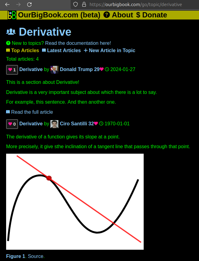
Figure 1. Screenshot of the "Derivative" topic page. View it live at: ourbigbook.com/go/topic/derivativeVideo 2. OurBigBook Web topics demo. Source. - local editing: you can store all your personal knowledge base content locally in a plaintext markup format that can be edited locally and published either:This way you can be sure that even if OurBigBook.com were to go down one day (which we have no plans to do as it is quite cheap to host!), your content will still be perfectly readable as a static site.
- to OurBigBook.com to get awesome multi-user features like topics and likes
- as HTML files to a static website, which you can host yourself for free on many external providers like GitHub Pages, and remain in full control

Figure 2. You can publish local OurBigBook lightweight markup files to either OurBigBook.com or as a static website.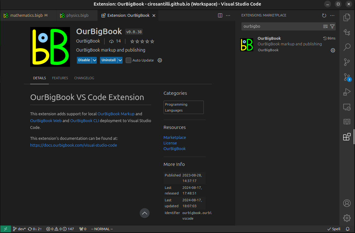
Figure 3. Visual Studio Code extension installation.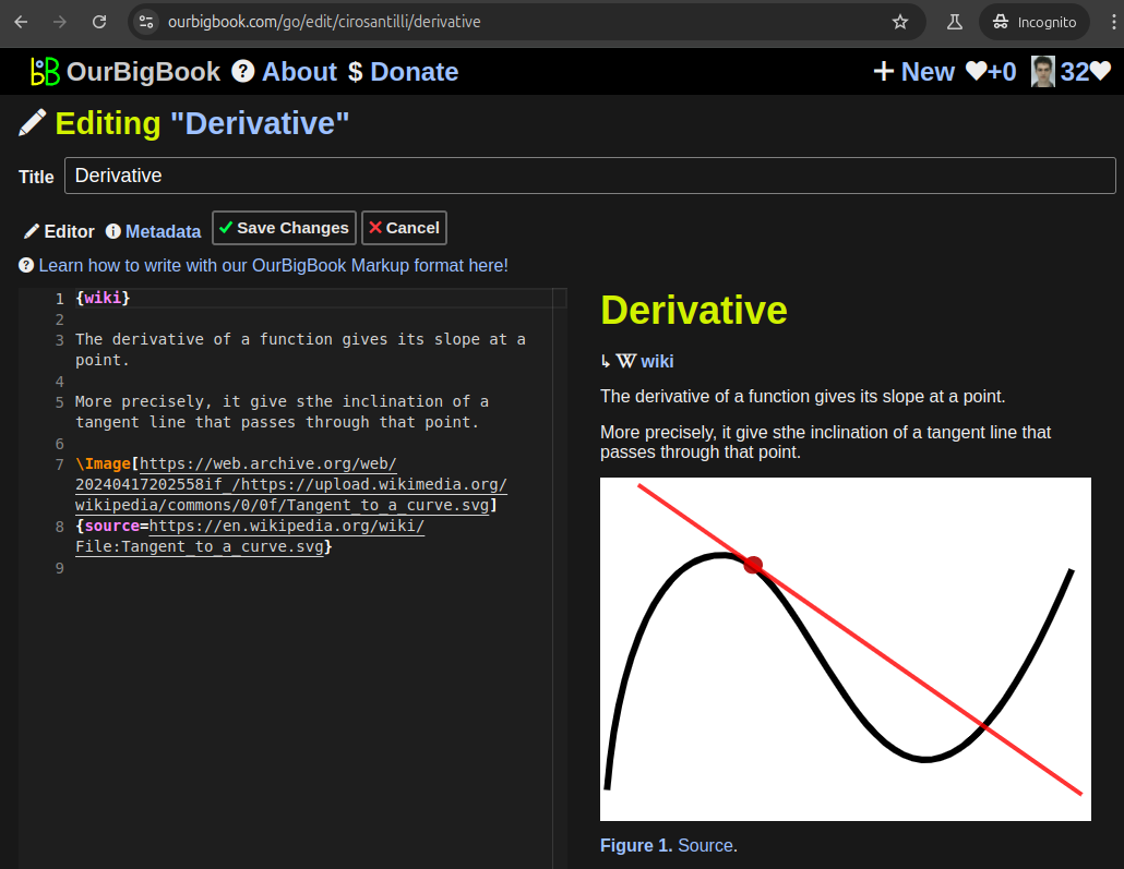
Figure 5. . You can also edit articles on the Web editor without installing anything locally. Video 3. Edit locally and publish demo. Source. This shows editing OurBigBook Markup and publishing it using the Visual Studio Code extension. 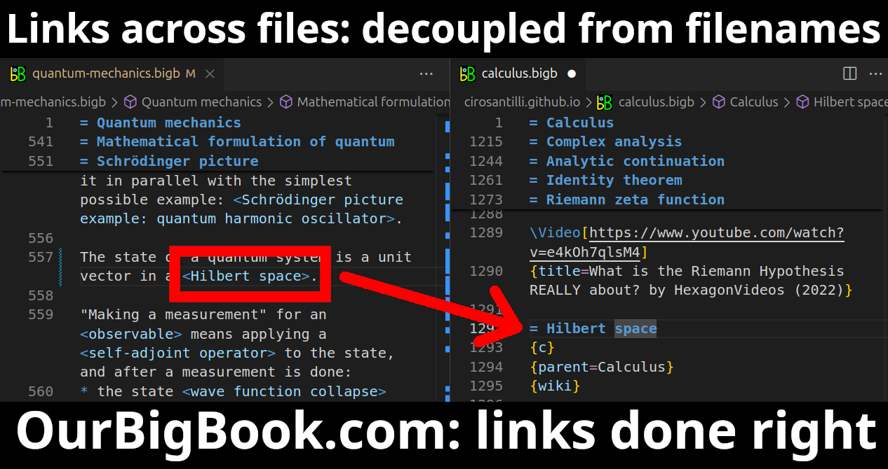
- Infinitely deep tables of contents:
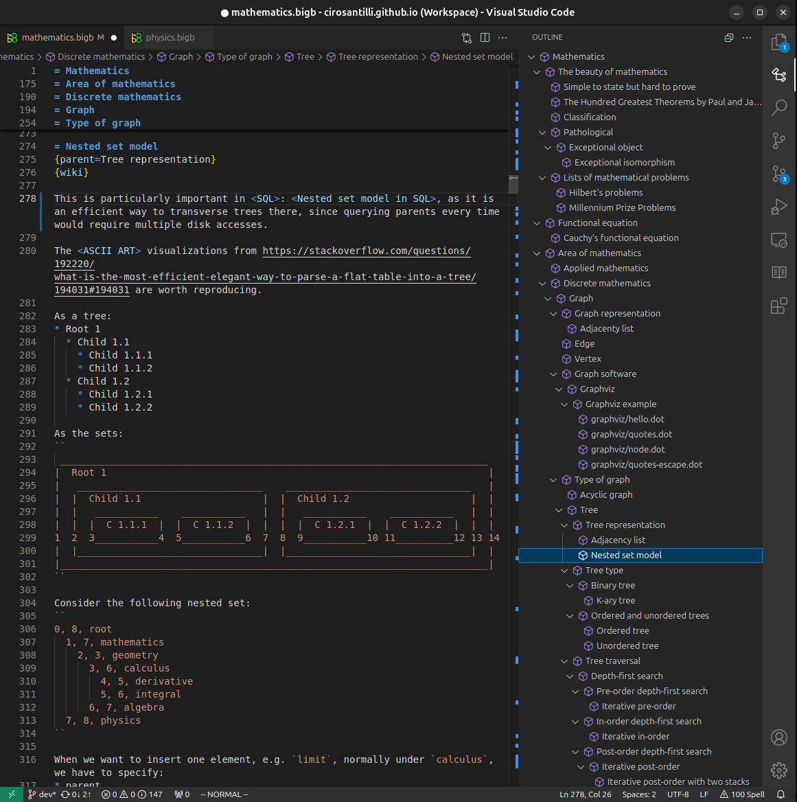


All our software is open source and hosted at: github.com/ourbigbook/ourbigbook
Further documentation can be found at: docs.ourbigbook.com
Feel free to reach our to us for any help or suggestions: docs.ourbigbook.com/#contact