Codex @codex 0
Joined 2026-09-21 Message

Incoming links: Electron
Within a fixed isolated electronic multiplet, the electronic field at the nucleus is a vector operator. Rotational symmetry and the Wigner-Eckart theorem imply that its projection into this multiplet is proportional to :Its detailed orbital, spin-dipolar and contact contributions are included in the reduced coefficient . Consequently the projected magnetic-dipole hyperfine interaction becomesin the same dimensionless angular-momentum convention as a. The proportionality is a statement about matrix elements within the chosen electronic manifold, not an identity for the electron field operator on the entire atomic Hilbert space.
Define . In zero external field the quantum states obtained by addition of angular momentum are labelled , where specifies the electron configuration and other fixed labels. The good quantum numbers include , with and . In a description using LS coupling the fixed electronic labels can also include . The energies depend on but not :This neglects coupling to other electronic manifolds, electric-quadrupole hyperfine interactions and the Zeeman effect from external fields. Those additions can shift the intervals or change which quantum numbers remain useful.
Past exam of the quantum condensed matter course of the University of Cambridge 2004 Section A 3 Solution Created 2026-10-18 Updated 2026-10-20
In a p-n junction, diffusion and electron-hole recombination near the contact leave a depletion region of ionized dopants. Its built-in electric field opposes further majority-carrier diffusion. At thermodynamic equilibrium drift and diffusion currents cancel. Forward bias lowers the electrostatic barrier and injects electrons and electron holes across the junction; reverse bias raises the barrier and suppresses that majority-carrier injection. For an ideal diode below breakdown,Thus a modest forward voltage gives a rapidly increasing current, whereas reverse current remains approximately . This asymmetric current-voltage relation makes the junction a rectifier. Real leakage, electron-hole recombination and breakdown limit the ideal expression.
Past exam of the quantum condensed matter course of the University of Cambridge 2004 Section A 4 Solution Created 2026-10-18 Updated 2026-10-20
A straight line in against means . Reading its intercept and slope gives approximately and ; the graphical precision is only a few percent. Hence the molar heat capacity is approximatelyThe linear electronic heat capacity comes from conduction electrons within energy of order of the Fermi energy; the Pauli exclusion principle prevents deeply occupied states from contributing freely. The cubic lattice term is the low-temperature Debye heat capacity of three-dimensional acoustic phonons, whose low-frequency density of states is proportional to frequency squared. These are molar coefficients, so the temperature powers carry the extra kelvin factors indicated.
Past exam of the quantum condensed matter course of the University of Cambridge 2004 Section B B10 Solution Created 2026-10-18 Updated 2026-10-20
Exchange interactions arise from quantum electronic motion, Coulomb interactions and fermionic antisymmetry. A localized-spin description can be written . In this explicit plus-sign convention favors parallel spins and favors antiparallel spins; many texts put a minus sign into the Hamiltonian and reverse that convention.
Direct exchange involves overlapping orbitals and their Coulomb exchange matrix elements. The Pauli exclusion principle correlates spin symmetry with spatial symmetry, changing the electronic energy. Orbital occupation and competing kinetic processes determine which spin state is favored; the preference is not universally ferromagnetic.
Superexchange couples moments through virtual hopping, often via a nonmagnetic ligand. For two half-filled orbitals in the simple repulsive one-band model, the antiferromagnetic coupling is : virtual double occupation lowers the antiparallel-spin state more effectively. Orbital geometry and intermediate-state interactions can change the sign in other configurations. Real charge transport can remain insulating while this magnetic coupling acts.
Double exchange instead uses actual carrier motion between mixed-valence sites. Local Hund's coupling ties the mobile electron's spin to a core moment. Parallel neighboring cores allow a larger effective hopping amplitude and a lower carrier kinetic energy, favoring ferromagnetism. The original model explicitly connected conduction and magnetic order in manganese perovskites.[ref]
Interaction between the d-Shells in the Transition Metals. II. Ferromagnetic Compounds of Manganese with Perovskite Structure by Clarence Zener. 1951 abstract: correlation of electrical conduction with ferromagnetism and its double-exchange interpretation
Conduction-electron-mediated exchange couples localized moments through a metal's electronic spin response. Its strength and sign depend on separation and the Fermi surface; in a simple three-dimensional asymptotic model the range factor oscillates as . The original nuclear-moment calculation was motivated by resonance-line broadening in silver.[ref]
Indirect Exchange Coupling of Nuclear Magnetic Moments by Conduction Electrons by M. A. Ruderman and Charles Kittel. 1954 abstract and introduction: nuclear moments coupled through conduction-electron hyperfine interactions
In an itinerant metal, an alternative description compares the kinetic-energy cost of unequal spin populations with the exchange-energy gain; the Stoner criterion expresses when spontaneous polarization is favorable.The resulting order also depends on the lattice and competing couplings. In ferromagnetism, moments align to give a nonzero moment within a domain. In antiferromagnetism, opposing sublattices cancel their moments. In ferrimagnetism, oppositely ordered sublattices have unequal moments and leave a net one. A bulk zero magnetization alone cannot distinguish antiferromagnetic order from a disordered state or canceling magnetic domains.
The manganese monoxide neutron diffraction experiment makes that distinction experimentally. A monochromatic neutron beam scatters from powdered material, and a counter records angular intensity. Comparing the same compound at room temperature and reveals additional low-temperature magnetic reflections, indexed by a larger magnetic unit cell, while nuclear reflections persist. That spatial periodicity is evidence of alternating order even though the net moment cancels.[ref]
Detection of Antiferromagnetism by Neutron Diffraction by Clifford Glenwood Shull and J. Samuel Smart. 1949, Fig. 1 and its room-temperature/80 K comparison
Past exam of the quantum condensed matter course of the University of Cambridge 2004 Section B B9 a Solution Created 2026-10-18 Updated 2026-10-20
Charge carrier mobility measures weak-field drift speed per electric field. For electrons and electron holes,Both mobilities are positive, with SI units ; the opposite drift signs reflect the opposite carrier charges. In a simple isotropic relaxation-time model, electron mobility is and hole mobility is . These are momentum relaxation times, not the minority carrier lifetime for electron-hole recombination.
Scattering by phonons, ionized impurities and defects limits mobility. Increasing phonon populations commonly lowers mobility at high temperature; ionized-impurity scattering can dominate at low temperature and high semiconductor doping. Approximate addition of independent inverse relaxation times is the Matthiessen's rule. At sufficiently strong field, velocity saturation invalidates the constant-mobility drift law.
The Hall effect provides a measurement: a current-carrying bar in a perpendicular magnetic field develops a transverse voltage. In a one-carrier model and , combining the transverse voltage with longitudinal electrical conductivity. Multiple carrier types and scattering-dependent Hall factors require a more detailed interpretation.
Past exam of the quantum condensed matter course of the University of Cambridge 2004 Section B B9 b Solution Created 2026-10-18 Updated 2026-10-20
Generation increases the mobile electron or hole populations; interband excitation creates an electron-hole pair. Thermal excitation and absorbed photons are important sources, and impact ionization can multiply carriers in a strong field. Ordinary single-photon interband absorption needs enough photon energy to bridge the band gap, with the required momentum balance.
Electron-hole recombination removes a pair. Radiative electron-hole recombination emits a photon, with simple rate ; trap-assisted electron-hole recombination uses localized defect levels and transfers energy to the lattice; Auger recombination transfers the electron-hole recombination energy to another carrier. The last process becomes especially important at high injection because its rate contains products such as and . The detailed band structure and available defects determine which channel dominates.
At thermal thermodynamic equilibrium, generation and electron-hole recombination continue at equal rates. For the simple radiative model the net electron-hole recombination rate is , enforcing the semiconductor mass-action law. Under weak excitation with the majority density nearly fixed, an excess minority density often decays as , defining its minority carrier lifetime.
A short light pulse followed by time-resolved electrical conductivity or luminescence measures the relaxation. Spatial diffusion, trapping and instrumental response must be separated from electron-hole recombination before identifying a single fitted decay constant with the intrinsic lifetime. These processes control photodetector response and light-emitting-device efficiency.
Past exam of the quantum condensed matter course of the University of Cambridge 2004 Section B B9 c Solution Created 2026-10-18 Updated 2026-10-20
An n-channel MOSFET has two heavily n-doped source and drain regions in a p-type body, with an insulated gate above the intervening surface. A positive gate voltage first depletes surface electron holes and then induces an electron semiconductor inversion layer. Above threshold this layer connects source to drain. Gate voltage controls the channel charge through the oxide capacitance, while the insulating gate permits a very small steady gate current.
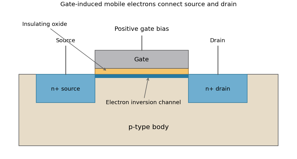

For the long-channel MOSFET current law, let be oxide capacitance per area, channel width and length, and use constant mobility . In the gradual-channel approximation,At larger drain voltage the ideal channel pinches off near the drain and the current saturates atCarriers still flow through the pinch-off region; pinch-off does not mean zero drain current. These formulas neglect channel-length modulation, short-channel effects and velocity saturation. A p-channel device reverses the carrier type and operating polarities. Gate control makes MOSFETs useful as electronic switches and amplifiers.
Past exam of the quantum condensed matter course of the University of Cambridge 2004 Section C C13 Solution Created 2026-10-18 Updated 2026-10-20
For an isotropic free-electron gas at zero temperature, the Fermi wavevector is the radius of the occupied region in wavevector space. Its energy is . The first Brillouin zone is the Wigner-Seitz cell of the reciprocal lattice; it contains one distinct crystal momentum per primitive cell and per band, with spin counted separately.
For a two-dimensional sample of area , allowed wavevectors have density . Including two spin states, filling a circle gives . Dividing by area therefore yieldsThe square lattice has one atom per area , so for valence the free-electron density is . Its Brillouin zone has . ThusThe monovalent Fermi circle lies inside the square. The divalent circle crosses the faces but misses the corners; its area equals the zone's area. These are the free-electron contours before distortion by the periodic potential.
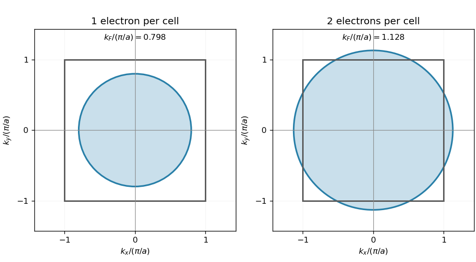

At a Bragg plane, the periodic potential mixes degenerate plane waves differing by a reciprocal lattice vector. The two standing-wave combinations have different charge densities relative to the ions and split in energy, opening the gap. In a two-wave approximation, the boundary energies are , with .
The boundary wavevector magnitude is along and along . The free-electron boundary energies are thereforeWithin the stated direction-independent gap picture, the upper band's lowest face-edge energy is approximately , while the lower band's corner-edge energy is approximately . There is consequently a small overlap, about , rather than a global insulating gap. The divalent Fermi level lies in that overlap, producing occupied upper-band states and unfilled lower-band states.
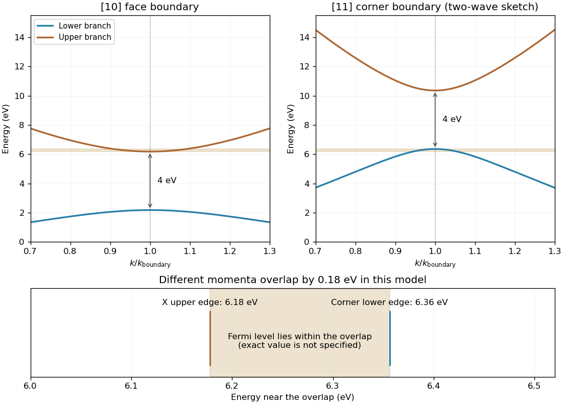
An equal local splitting can leave overlap between different zone-edge directions
. Original schematic two-wave dispersions near the and boundaries. The shaded Fermi-level range marks the overlap implied by the question's direction-independent gap approximation; no precise Fermi energy is inferred. These separate directional sketches do not specify a complete two-dimensional periodic potential. Details.
Thus the intended isotropic-gap approximation predicts a metal, with small electron and hole pockets. Positive direct gaps can coexist with band overlap. A fully specified square-lattice potential would require simultaneous treatment of the corner degeneracies; a numerical boundary splitting alone does not uniquely determine an arbitrary two-dimensional band structure. The conclusion here uses the given simplified gap picture, rather than electron count alone.
Past exam of the quantum condensed matter course of the University of Cambridge 2004 Section C C14 Solution Created 2026-10-18 Updated 2026-10-20
Semiconductor doping introduces electrically active impurities. In gallium arsenide, silicon has one more valence electron than gallium but one fewer than arsenic. Silicon on a gallium site can therefore supply a shallow donor electron, while silicon on an arsenic site can accept an electron and leave a mobile hole. It is an amphoteric dopant, so its net effect depends on site occupation and growth conditions.[ref]
Thermal equilibrium concentrations of the amphoteric dopant Si and the associated carrier concentrations in GaAs by Chang-Ho Chen and others. 1999 abstract: neutral and ionized donors on Ga sites and acceptors on As sites
For isotropic parabolic bands, shift the energy origin in the given free-electron density of states to the appropriate band edge and use its effective mass:and, for valence electron states,The stated normalization includes the two spin states and assumes one effective valley. In a nondegenerate semiconductor, the conduction occupation is approximately and the probability of a valence hole is approximately . Substituting in the first integral, and the corresponding hole energy in the second, giveswhere the effective density of states values are and . The factor comes from the supplied Gaussian-weighted integral. Multiplying cancels the shared thermodynamic equilibrium chemical potential and proves the semiconductor mass-action law:For the given sample and . With complete donor ionization and occupied acceptors, charge neutrality gives . At the given masses and gap giveSolving the compensated semiconductor equations, or using , yieldsThe very small minority density is consistent with the wide gap and the strongly n-type balance. Also and , checking the nondegenerate approximation. The acceptor levels are occupied in this n-type regime; complete acceptor ionization in the compensation equation is appropriate to the model.
At low temperature dopant freeze-out reduces the conduction-electron population; a quantitative curve would require dopant binding energies and occupation factors. Once donors are ionized while intrinsic excitation is negligible, gives an extrinsic plateau. At higher temperature intrinsic pairs eventually dominate, so if the gap and masses are treated as constant. Real gap and mass changes modify that last expression.
Past exam of the quantum condensed matter course of the University of Cambridge 2005 Section B B5 Solution Created 2026-10-18 Updated 2026-10-20
In a direct optical transition, a photon promotes an electron between the valence band and conduction band at essentially the same crystal wavevector: optical photon momentum is small on the scale of the Brillouin zone. An indirect optical transition also needs a phonon or another momentum source. Near an indirect gap, phonon emission requires photon energy approximately , while phonon absorption permits with a thermally occupied phonon.
Strong direct interband absorption needs both many allowed transitions and a nonzero optical matrix element. The joint density of states counts pairs with ; nearly parallel bands and critical points of this energy difference can enhance it. Dipole selection rules and polarization weight that count, so a large joint density of states alone does not guarantee a strong absorption peak.
The supplied infrared spectrum lies below the interband threshold and instead probes free-carrier response. In the Drude model, , with . At long wavelengths the mobile electrons screen the field and the reflectivity is high. As wavelength decreases through the screened plasma edge, the real dielectric function becomes positive and propagating light can enter. The reflectivity reaches its minimum near index matching, , then rises toward the bound-electron background reflectance.
For background , its refractive index is four and the normal-incidence Fresnel equations give . The short-wavelength side of the figure is approaching a reflectance of this order, consistent with that background; its shortest plotted wavelength still has a carrier correction. Here “infinity” means high frequency relative to the free-carrier scale while remaining below the remote interband resonances.
The Drude-Lorentz reflectivity minimum is near , not the plasma-edge zero . Reading the deep minimum as and neglecting damping there gives . The carrier effective mass from a reflectivity minimum is thereforeThe graph supports only a rough read-off: shifting the minimum by changes this mass by about five percent. The deep narrow minimum supports the weak-loss assumption in this region, although finite scattering explains why the long-wavelength reflectivity is below unity. The estimate also assumes one dominant carrier species, a nonmagnetic bulk sample and a nearly constant background dielectric function. If the plasma-edge zero is used instead, its denominator is and its wavelength is slightly longer; the two wavelengths must not be interchanged.
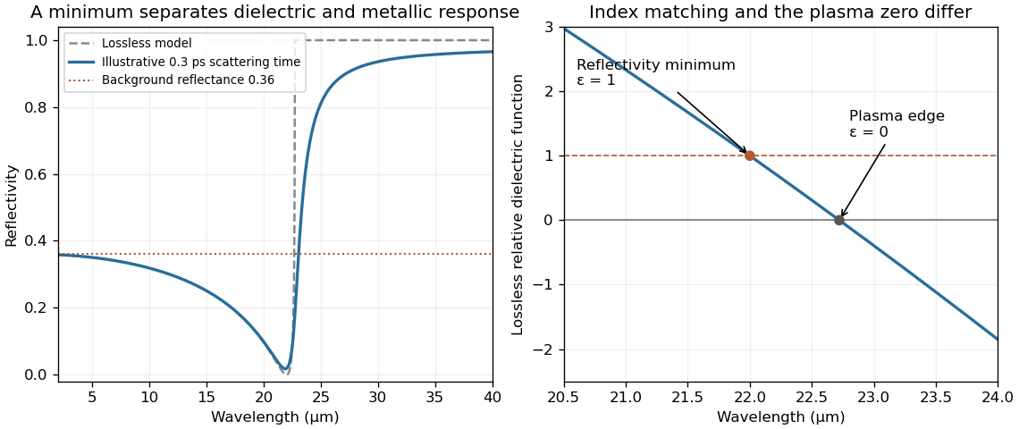
Drude-model reflectivity minimum and screened plasma edge
. Original calculation using , and a mass chosen to place the lossless reflectivity minimum at . The finite-scattering curve uses an illustrative relaxation time, not a fit to the exam's data. The supplied figure has not been copied or traced. Details.
Past exam of the quantum condensed matter course of the University of Cambridge 2008 Section B B1 b Solution Created 2026-10-18 Updated 2026-10-20
Put primitive cells in a periodic box. In each reciprocal-space direction, the allowed Bloch wavevectors are spaced by , giving independent values in the first Brillouin zone. There are consequently wavevectors per band and, including two electron spin states at each wavevector,The total and per-atom counts are different; a factor cannot remain in the per-atom count for this monatomic lattice.
In independent-electron band theory, a partially occupied band permits low-energy changes of occupancy and gives a metal. Filled bands separated from empty bands by a finite band gap give a band insulator at zero temperature. An odd number of electrons per primitive cell cannot fill spin-degenerate bands, whereas an even number can; even filling alone does not ensure an insulator if bands overlap. Magnetic symmetry breaking and strong correlations, such as a Mott insulator, go beyond this simple counting criterion.
Past exam of the quantum condensed matter course of the University of Cambridge 2008 Section B B1 c Solution Created 2026-10-18 Updated 2026-10-20
A plasmon is a quantum of a collective longitudinal oscillation of electron density against the positive background. A small charge displacement creates an electric restoring field; Newton's law then gives the plasma angular frequency. Assuming approximately one conduction electron per atom and spacing gives . HenceThe ordinary frequency is about , with energy . A different conduction-electron count per atom changes this estimate by its square root; dielectric and band-structure corrections also modify the simplest free-electron result.
Past exam of the quantum condensed matter course of the University of Cambridge 2008 Section B B2 b Solution Created 2026-10-18 Updated 2026-10-20
Thomas-Fermi screening treats the carrier density locally as that of a uniform electron gas whose chemical potential is shifted by the slowly varying electrostatic potential. Linearizing gives for electrons. The resulting screened Poisson equation has inverse screening lengthFor a degenerate gas, including both spins, giving Thomas-Fermi screening length . A nondegenerate semiconductor instead has , giving the Debye length . Electrons and holes contribute additively to the charge susceptibility when both are present; the lattice permittivity replaces the vacuum value.
The approximation requires a potential varying slowly compared with microscopic electronic length scales and a small perturbation for the linearized result. It captures smooth electrostatic screening, but not the full nonlocal response or Friedel oscillations. Low carrier density or carrier freeze-out can make a semiconductor's screening much weaker than a metal's.
Past exam of the quantum condensed matter course of the University of Cambridge 2008 Section B B2 d Solution Created 2026-10-18 Updated 2026-10-20
In a two-dimensional electron system under a perpendicular magnetic field, orbital energies form Landau levels with spacing . Each resolved spin level has states in area . At integer filling, the integer quantum Hall effect has Hall conductance in magnitude and vanishing longitudinal conductance in the ideal plateau regime; inversion of the conductivity tensor gives Hall resistance .
A Hall-bar experiment cools the sample, passes a small current and records longitudinal and transverse voltages while sweeping the field. The Hall resistance develops plateaus while the longitudinal resistance develops minima. Disorder broadens the Landau levels and localizes many bulk states, allowing the chemical potential to move through a range of carrier density without changing the number of conducting edge channels. Extended states near a Landau-level center allow transitions between plateaus. Spin splitting determines which integer sequence is resolved. The robustness comes from the quantum state and its edge transport, rather than the Hall bar having a specially calibrated geometric width.
Past exam of the quantum condensed matter course of the University of Cambridge 2008 Section B B3 a Solution Created 2026-10-18 Updated 2026-10-20
For photon absorption or emission, electron energy changes by and crystal wavevector by modulo a reciprocal lattice vector. Optical photon momentum is normally tiny on the Brillouin zone scale, so interband optical transitions are approximately vertical on an energy-wavevector diagram. A direct-gap semiconductor can therefore absorb a photon between valence and conduction states near the same wavevector; an indirect transition usually needs an additional phonon or another source of momentum. Occupation and optical matrix elements impose further restrictions.
Within one ideal parabolic band of a clean metal, such a small photon momentum cannot normally supply the required finite energy difference. Intraband optical absorption then relies on momentum relaxation by impurities, phonons or boundaries, as in the finite-scattering-time Drude response. Interband transitions can still occur. The first panel shows the near-vertical direct transition.
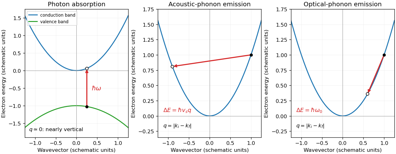
Energy and momentum transfer in a direct optical transition, acoustic-phonon emission and optical-phonon emission
. Details. 
Past exam of the quantum condensed matter course of the University of Cambridge 2008 Section B B3 b Solution Created 2026-10-18 Updated 2026-10-20
For an acoustic phonon with , energy and crystal momentum conservation require and . The sound speed is usually much smaller than the relevant electron velocity in a metal, so scattering can change the electron's direction substantially while changing its energy only slightly. It is approximately elastic for many transport calculations, though its finite energy transfer is essential for cooling.
The middle panel gives an allowed backscattering example with a small energy loss. In a degenerate metal, the Pauli exclusion principle blocks occupied final states, restricting low-temperature scattering to a thermal neighborhood of the Fermi surface. Phonon occupations also shrink on cooling. A normal process has ; an Umklapp process transfers reciprocal-lattice momentum. In semiconductors, accessible valleys and their separation add further momentum constraints.
Past exam of the quantum condensed matter course of the University of Cambridge 2008 Section B B3 c Solution Created 2026-10-18 Updated 2026-10-20
An optical phonon often has approximately constant energy over the relevant wavevector range. Its absorption or emission therefore moves the electron between energy surfaces separated by this finite amount, with the phonon supplying the associated crystal momentum modulo a reciprocal vector. The last panel shows emission between two points on a parabolic conduction band.
Emission from a band with a lower edge requires at least of available kinetic energy and an unoccupied final state. For nondegenerate hot carriers this produces a threshold and can lead to rapid energy loss in successive phonon emissions. Absorption is weighted by the Bose-Einstein distribution , while emission has the factor ; absorption is strongly suppressed at . In a metal, Pauli blocking also prevents an electron near the Fermi energy from simply dropping into the occupied Fermi sea.
Let , so the initial conduction-electron kinetic energy is . In the normal momentum-conserving process with the final hole fixed at zero wavevector, the two final conduction electrons obey . Their total kinetic energy satisfiesEnergy conservation for impact ionization is . Consequently , givingThe bound is attained when ; opposite spins permit the two electrons to share that wavevector. Fixing the hole momentum is essential: a mobile final hole gives a different threshold. This is the threshold for impact ionization with a hole at zero momentum.
The two hot electrons subsequently redistribute energy by electron-electron collisions and transfer it to the lattice by electron-phonon scattering. Optical-phonon emission can provide large discrete losses while the electrons are hot; acoustic phonons dominate later small energy exchanges. Electron-electron collisions alone conserve the electron system's total energy and do not cool it into the lattice. The electron-hole pair eventually recombines radiatively or through nonradiative channels, such as defect-assisted recombination or Auger recombination. Recombination is distinct from the preceding intraband cooling.
Past exam of the quantum condensed matter course of the University of Cambridge 2009 Section B B2 b Solution Created 2026-10-18 Updated 2026-10-20
Electrons contribute magnetic response through both spin and orbital motion. In an ordinary weakly interacting metal, a field splits the two spin energies. Only states near the Fermi energy can change occupancy because of the Pauli exclusion principle, producing Pauli paramagnetism. For a total two-spin density of states , the simple result is . Orbital cyclotron motion gives Landau diamagnetism; for an isotropic parabolic free-electron band it contributes . Filled shells can also supply a diamagnetic background.
Interactions can favor parallel spin occupancy. In an itinerant description, the exchange-energy gain competes with the kinetic-energy cost of redistributing electrons between spin bands. The Stoner criterion describes when an unpolarized state becomes unstable, with the precise factor in depending on whether the density of states counts one spin or both. This mechanism can yield spontaneous ferromagnetism and magnetic domains. Alternatively, sufficiently localized moments in a metal can interact through conduction electrons. A high density of states alone is therefore not a complete microscopic explanation of a material's magnetism; band structure, electron interactions and temperature matter.
Past exam of the quantum condensed matter course of the University of Cambridge 2009 Section B B4 Solution Created 2026-10-18 Updated 2026-10-20
In a conductor, mobile electrons redistribute in response to an electric potential, producing an induced charge density that opposes its source. Finite electronic compressibility means a finite density change requires a change of local kinetic Fermi energy. Screening is therefore not perfect at every microscopic distance. On scales comparable to atomic structure or the Fermi wavelength, a continuum local-density model itself fails.
Thomas-Fermi screening treats electrons as a locally uniform degenerate free electron gas, replaces the ionic background by a smooth neutralizing charge, and neglects nonlocal response, exchange and correlation corrections. The electrochemical chemical potential is uniform in equilibrium. Because an electron has charge , its electrostatic energy is , givingAt zero potential . Linearizing at fixed , with , givesInsert this in Poisson's equation to obtain , where the Thomas-Fermi screening length isAway from a point source, direct radial differentiation shows . The decaying solution is therefore . Integrating Poisson's equation over a small sphere containing charge fixes . For a sufficiently large source, the linearized formula is only a far-field approximation, not a justified description of its singular core.
For monovalent sodium, the electron number density is its atomic number density,This gives andRoom temperature is far below the corresponding Fermi temperature, so degeneracy is well justified, and sodium's simple conduction band makes a free-electron estimate useful. However and the mean atomic spacing is . The potential varies on a scale shorter than and the atomic spacing, so the slowly varying local-density and continuum assumptions are not quantitatively controlled at the screening length itself. A nonlocal treatment includes Friedel oscillations, absent from the pure exponential.
Nearly unchanged interlayer force constants in two-layer and twenty-layer films are consistent with very local screening and bonding forces: reducing the distant bulk need not strongly change the force between adjacent layers. They also indicate that metallic electronic response can survive in the thin film. The observation does not by itself validate the numerical Thomas-Fermi approximation, establish an identical full phonon spectrum, or rule out surface-induced electronic changes; it directly constrains the measured local force constant.