
Interferogram 2026-10-18
An interferogram records detected light intensity produced by interference as a controlled position, phase or delay is varied. In Fourier transform spectroscopy, the variable is the delay between two copies of the same field. Removing the constant background gives a correlation signal whose Fourier transform determines the source's spectral power density, subject to the measured delay window and instrumental response.
Division of amplitude 2026-10-18
In division of amplitude, a partially reflecting interface sends parts of the same incident wavefront into separate paths that are later recombined. A Michelson interferometer is an example. The resulting interference visibility depends on relative optical path length, polarization of waves, intensity balance and optical coherence.
Division of wavefront Created 2026-10-18 Updated 2026-10-20
In division of wavefront, different spatial portions of an incident wavefront are selected and propagated so that their fields overlap. Double-slit interference is an example. The selected portions need sufficient spatial optical coherence for stable interference fringes.
Beat Created 2026-10-18 Updated 2026-10-25
The slow change in the resultant amplitude when two nearby frequencies interfere. Two steady sinusoidal components at and produce successive amplitude maxima separated by .
Phase matching 2026-10-18
A relation between wave phases that lets contributions from successive interaction regions add coherently. In Cherenkov radiation, the condition along the particle trajectory is , relating angular frequency, wave vector and particle velocity.
Double-slit experiment 2026-10-18
The double-slit experiment compares propagation through two openings. Coherent illumination gives double-slit interference; independent incoherent source patches contribute light intensities whose displaced patterns can reduce the observed interferometric visibility.
Thin-film interference 2026-10-18
Thin-film interference combines coherent light contributions reflected or transmitted at the two surfaces of a layer. For a film of refractive index , thickness and internal angle , the round-trip optical path difference is . The relative reflection phase shift must also be included. For a nonabsorbing higher-index film surrounded by air, one of the two leading reflected contributions has a phase shift and the other does not. Reflection maxima therefore satisfy . A smooth reflection spectrum filters many visible wavelengths at once; varying thickness and angle produce spatially varying mixed colours.
Destructive interference 2026-10-18
Destructive interference occurs when coherent contributions partially or completely cancel their complex amplitudes. For two equal contributions, a phase difference of modulo gives zero resultant wave amplitude. The missing local light intensity is consistent with conservation of energy because the full spatial interference pattern redistributes power.
Moiré pattern Created 2026-10-18 Updated 2026-11-05
A Moiré pattern is a large-scale modulation produced by superposing similar periodic structures. Two identical two-dimensional lattices rotated by a small angle have geometric period in the usual matching geometry. In layered crystals this modulation can act as an electronic superlattice; the actual bands additionally depend on interlayer coupling and orbital structure.
Poisson defect yield 2026-10-18
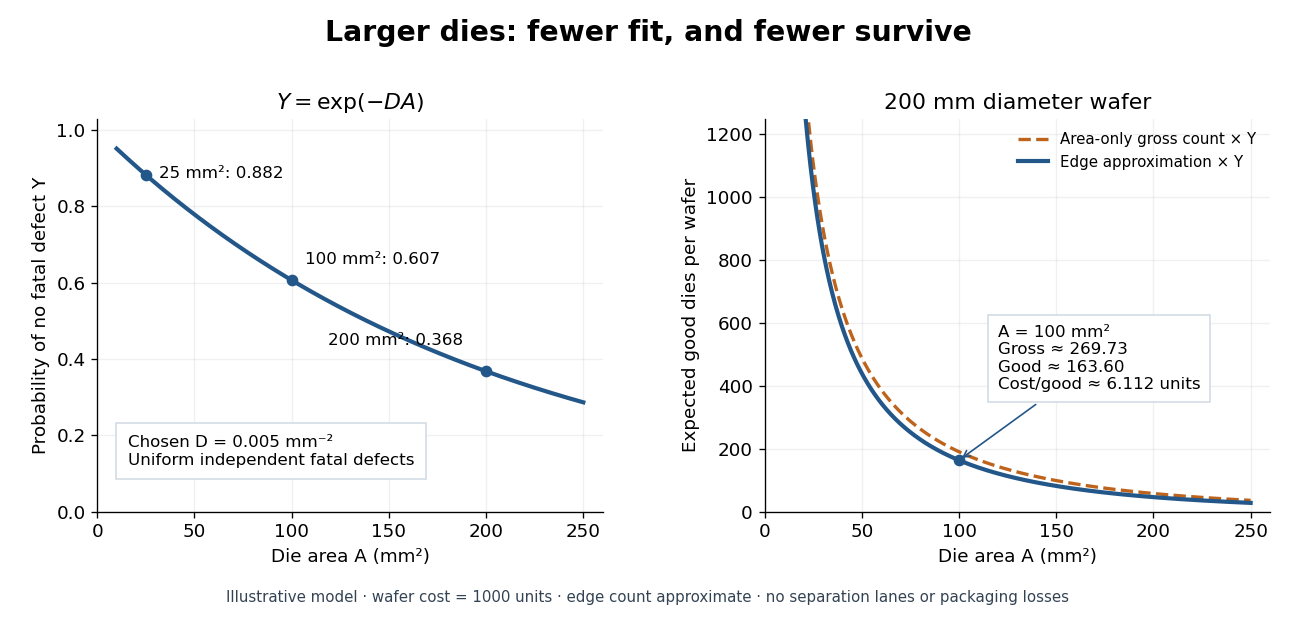
Consider a deliberately simplified model: fatal defects form a spatially uniform Poisson point process with intensity per unit area. A semiconductor die of area works exactly when it contains no fatal defect. Its defect count has a Poisson distribution with expected value , hence its probability of working, called its yield, isThe product is dimensionless. The formula concerns fatal defects, not every visible imperfection. Spatial uniformity, independent defect counts in disjoint areas, and failure from even one fatal defect are model assumptions. Clustering, shared processing failures, repairable regions and defects that affect only some functions can invalidate them. This is a chosen probability model, not historical yield data.
Choose . For semiconductor die areas , and , the model gives , and . Doubling the area squares the yield: . This follows either from the exponential function or by splitting the larger area into two disjoint parts and using independence. More functions on one semiconductor die can save assembly while making the no-defect requirement harder to satisfy.

Semiconductor wafer 2026-10-18
A thin piece of semiconductor processed to form devices or integrated circuits, often many semiconductor dies together. Dividing wafer area by die area gives an ideal count before edge losses and spaces used to separate semiconductor dies.
Integrated circuit interconnect 2026-10-18
An integrated circuit interconnect is a conducting path joining circuit regions. In Robert Noyce's patent, deposited metal strips cross retained oxide on silicon; selected openings permit contact to the semiconductor while oxide prevents unwanted contact across p-n junctions. Figs. 3–5 combine detection, filtering and electronic amplifier functions using a transistor in one structure. The key is both connectivity and insulation: a metal path must touch its intended terminals while crossing other regions without shorting them.[ref]
Semiconductor device-and-lead structure by Robert Noyce. Description of Figs. 1–5, oxide tongues, metal strips and integrated circuit; claim 1
Planar process 2026-10-18
The planar process fabricates semiconductor devices from a common surface while retaining a protective oxide over the exposed ends of their p-n junctions. Jean Hoerni's patent describes selective openings in silicon dioxide for semiconductor doping and contacts, with oxide left over the p-n junctions. Protection and access are designed together; the surface is not simply stripped after fabrication. This was a distinct enabling contribution to the monolithic integrated circuit.[ref]
Method of manufacturing semiconductor devices by Jean Hoerni. Description, opening problem statement and Figs. 6–10, masking, retained oxide and contact openings
Kilby integrated circuit demonstration 2026-10-18
In his 2000 lecture, Jack St. Clair Kilby describes an August 1958 comparison circuit made from separate silicon elements. Resistors were cut and etched; capacitors came from diffused, metallized semiconductor wafers. It tested whether semiconductor elements could perform all the required functions, but was still a discrete circuit. For the September prototype he used already diffused germanium material with contacts, cut into bars, and hand-applied wax masks to define a transistor and a distributed resistor-capacitor region. Applying supply power produced an oscillation.[ref]
Turning Potential into Realities: The Invention of the Integrated Circuit (Nobel Lecture) by Jack St. Clair Kilby. Kilby's 2000 Nobel lecture, ChemPhysChem reprint (2001), pp. 486–487, separate-element comparison and oscillator preparation
An inspected eyewitness interview describes the germanium on a microscope slide with protruding wires; changing its connections changed the oscilloscope display from a straight line to a sinusoid. This supplied a qualitative connected/disconnected comparison, not a calibrated record of amplitude, loading or repeatability.[ref]
Oral History of Jay W. Lathrop. Oral History of Jay W. Lathrop, recorded 7 May 2009, p. 11, demonstration and oscilloscope comparison
The inference was feasibility: integrated semiconductor elements could cooperate as an operating electrical circuit. The hand-wired germanium prototype did not yet supply the deposited integrated circuit interconnects of Robert Noyce's silicon design. Nor does a working prototype establish manufacturing yield or long-term reliability.
Monolithic integrated circuit 2026-10-18
A monolithic integrated circuit has its circuit elements fabricated in or on one semiconductor die. Their connections are essential: an unconnected collection of transistors does not implement the intended electrical circuit.
An original ideal example separates function from fabrication. Connect two resistors, above , in a series circuit across an ideal voltage source. With no load electric current drawn from their meeting point, Ohm's law and the Kirchhoff cycle law giveThese equations apply to either a discrete circuit or an idealized monolithic integrated circuit realizing those same electrical resistances. Integration changes construction; the electrical circuit equations still determine the output. A real load, unwanted capacitance or finite resistor tolerance changes the ideal calculation. Manufacturing many functions together also couples their fate: a fatal defect can discard an entire semiconductor die, motivating the Poisson defect yield model.
Discrete circuit 2026-10-18
An electrical circuit assembled from separately made components, such as individual transistors, resistors and capacitors. Several functions can share a package without forming a monolithic integrated circuit; packaging alone does not establish how the components were fabricated.
Transmembrane protein 2026-10-18
A transmembrane protein has at least one polypeptide chain crossing the complete lipid bilayer. One crossing is single-pass; several crossings in one chain are multipass. Hydrophobic regions face the membrane interior, while hydrophilic regions can face water.[ref]
Cell Membranes. The Cell: A Molecular Approach, 2nd edition by Geoffrey M. Cooper; Cell Membranes, Membrane Proteins: spanning regions, single and multiple crossings
Crista Created 2026-10-18 Updated 2026-10-20
A crista is a fold of the inner mitochondrial membrane into the mitochondrial matrix. Its membrane remains continuous with the surrounding inner mitochondrial membrane; it is not a separately inserted sac like a thylakoid.[ref]
Molecular Biology of the Cell, 4th edition by Bruce Alberts and others. Chapter 12, The Transport of Proteins into Mitochondria and Chloroplasts, Figure 12-22: continuity of cristae and contrast with thylakoids
The diagram idealizes access through the fold's opening. Connectivity alone does not imply instant mixing or identical concentrations throughout the intermembrane space. Narrow geometry and molecular interactions can matter to transport. Increasing surface area also does not, by itself, prove a proportional increase in ATP production: the supply of substrates, available oxygen and the state of the coupling machinery must also support the flux.
For the initially circular damped planar oscillator with overdamping , put . The exact solution replaces by . Resolving along the starting radius and its anticlockwise tangent yieldsIts limiting angle is the title value. Both coordinates remain positive when , so the trajectory returns to the origin without repeated revolutions. It initially moves tangentially and bends toward its slow decaying eigenmode, rather than following a radial straight line from the start.
Inductance of a toroid with an oblique narrow air gap Created 2026-10-18 Updated 2026-10-20
Let a slender toroid have core cross-section , mean length and large relative magnetic permeability . Cut a narrow gap of perpendicular width whose faces make angle with the local core direction. Continuity of normal magnetic flux density gives ; continuity of tangential magnetic field intensity gives . The gap field is nearly normal to the faces for large . Its effective flux area is , so its leading magnetic reluctance is . Adding core reluctance gives the displayed self-inductance. At , and . This retains while neglecting fringing and corrections of relative order or .
There are unlisted articles, also show them or only show them.