Official past-paper archive: www.sp.phy.cam.ac.uk/drp2/home. The direct PDF link has not yet been verified.
Use a representative conduction-electron density , roughly one mobile Electron per atom in a dense metal, and the bare Electron mass for this estimate. The plasma frequency is thenThis is an order-of-magnitude answer because no particular metal or carrier density is specified. It corresponds to an ordinary frequency , excitation energy , and free-space wavelength near .
The physical oscillation is collective motion of the electron gas against the positive ionic background. Displacing the Electrons relative to the ions produces a restoring electric field. In the simplest uniform-displacement picture, : the frequency increases with the density of mobile electric charge and decreases with carrier inertia. Quantizing this longitudinal collective oscillation gives a plasmon.
The same scale controls the ideal collisionless Drude model optical response. Its cold collisionless plasma dielectric response is . Below , the negative relative permittivity makes a transverse electromagnetic wave evanescent, producing strong reflection; above it, the ideal model admits propagation. Real-metal collisions, interband photon absorption and background polarization modify this simple optical edge. Thus is a collective charge-response scale, not a single-electron scattering rate or a sharp transparency threshold for every real metal.
Adopt the usual orthogonal tight-binding approximation, so the three localized spatial states are orthonormal. Each site has two neighbors, with the same real hopping matrix element. For coefficients , the Schrödinger equation at site isThe constant-coefficient state has , giving energy . Its normalization therefore yieldsTo verify that it is the ground state, the three discrete ring momenta are , with and energies . The other two states both have energy . Since , and the gap is . This is the three-site tight-binding ring spectrum.
The spatial ground state is unique and has equal probability on every site; its common overall phase is arbitrary. Spin would supply a separate twofold degeneracy when no spin-dependent terms are included, but does not change the requested spatial state. If the localized functions were instead nonorthogonal raw atomic orbitals, their overlap matrix would be additional data needed for normalization and a generalized eigenvalue problem.
The energy favoring spin polarization must compete with the increase in Fermi kinetic energy. Assume the usual three-dimensional zero-temperature parabolic conduction band at fixed and . Write the spin polarization as , so . The unpolarized Fermi energy isThe two spin populations have Fermi energies . Summing their individual mean kinetic energies givesThe specified interaction is an energy per Electron, . Thus the energy change per Electron near the unpolarized state isThe quadratic coefficient changes sign at the Stoner threshold for an interaction normalized per electron,The positive quartic term gives a continuous onset in this model. More globally, . Convexity of makes this nonnegative for , so no lower polarized minimum appears before that threshold.
At fixed number density , the critical is independent of the total sample size. A comparison restricted to a fully polarized state gives a different numerical coefficient, , but the same requested density scaling; it misses the partially polarized onset. One must also distinguish this , with units of energy, from a contact coupling multiplying an interaction-energy density : here . Importing a differently normalized Stoner criterion would introduce an erroneous extra density factor.
A covalent bond is stabilized by shared electronic states extending across neighboring atomic nuclei. In a simple two-centre description, combining comparable atomic orbitals produces a bonding state with enhanced electron density between the nuclei and an antibonding state with a node there. For equivalent normalized orbitals with real overlap ,Their energy ordering follows from the molecular Hamiltonian; constructive interference and reduced gradients help explain why the bonding combination can be lower. Opposite-spin Electrons can occupy the bonding orbital together. The familiar molecular-hydrogen bond is a basic example, while extended covalent networks form solids such as diamond. Orbital shape and hybridization make covalent bonding strongly directional and constrain bond angles. Occupying antibonding states reduces the net bond strength.
Ionic bonding instead emphasizes electric charge transfer and the electrostatic attraction of the resulting oppositely charged ions. Removing an Electron from one atom costs ionization energy and adding it to another gains electron affinity; these isolated-atom terms alone need not favor transfer. In a crystal, the electrostatic lattice energy can stabilize the ionic arrangement. For a schematic lattice of singly charged ions at nearest-neighbor distance ,where the geometrical Madelung constant sums attractions and repulsions throughout the lattice. Short-range overlap repulsion prevents collapse and gives an equilibrium separation. Sodium chloride is an example of an extended ionic crystal, rather than isolated NaCl molecules in the solid.
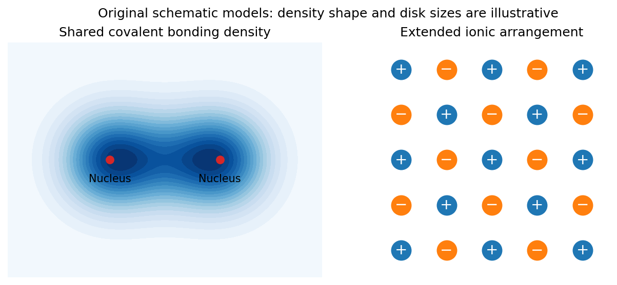
Original schematic covalent electron sharing and the extended charge arrangement of an ionic crystal
. Details. Ideal ionic bonding is comparatively nondirectional, so packing, ion sizes and electric charge balance strongly influence coordination. ions cannot freely migrate in the ordinary solid; melting or dissolution can make ionic electric charge transport possible. Covalent materials do not obey one universal electrical conductivity rule: their electronic bands and filling determine whether mobile electronic carriers are available.
The two descriptions are limiting models, not a sharp classification of every bond. Unequal electronegativities can produce polar covalent bonds with partial electric charge transfer, and a material may contain both covalent groups and ionic interactions between those groups. Chemical bonding reflects a balance of electronic kinetic energy, electron-nucleus attraction, electron-electron repulsion and nuclear repulsion; it cannot be reduced to a force between two assigned point charges in every material.
The Drude model treats mobile electric charge carriers as independent particles with density , signed electric charge , isotropic mass , and momentum relaxation time . In uniform steady fields,At zero magnetic field the drift velocity is , giving electrical conductivity and electrical resistivityThe electrical conductivity is positive for either carrier sign. Scattering dissipates directed drift energy into the environment; a finite steady electric current is compatible with a short-lived drift momentum. The independent-carrier relaxation-time approximation omits detailed band anisotropy, quantum interference and microscopic collision correlations.
For electric current along and magnetic field , the magnetic force deflects carriers toward one side of the sample. electric charge accumulates until a transverse Hall field cancels that force in an open transverse circuit. With , , soElectrons have negative in this convention, whereas positive carriers have positive . For a strip of thickness along , the magnitude of the Hall electric potential difference across its width is . Thus Hall measurements determine carrier sign and, within this one-carrier model, density, while combining with determines charge carrier mobility .
Keeping both in-plane electric current components, the resistivity tensor isThis fixes the off-diagonal sign convention and shows that inversion is not componentwise reciprocation. Under the Hall boundary condition , the ideal one-carrier isotropic model gives , independent of magnetic field: there is no ordinary longitudinal magnetoresistance in this minimal model. Multiple carrier types or anisotropic bands can change both this conclusion and the simple inference. Their electrical conductivity must be added before inverting to obtain the total electrical resistivity.
Both models respect Bloch's theorem and describe Electrons in a periodic lattice, but they start from different useful limits.
In the nearly-free electron model, start with extended plane waves and free-electron energies . A weak periodic potential has Fourier coefficients at reciprocal lattice vectors and couples to . Away from degeneracies its corrections are small. Near a Bragg scattering, retain the two resonant plane waves and diagonalizeThe resulting eigenvalues areAt the crossing the gap is . The two standing-wave combinations place electronic density differently relative to the periodic potential and therefore acquire different energies. Folding the many free parabolas into the first Brillouin zone produces the repeated band labels; the nonzero potential opens avoided crossings between coupled states. A Fourier component forbidden by symmetry need not open its corresponding first-order gap.
In the tight-binding model, instead start with localized orbitals on well-separated atoms or sites, with discrete on-site energies. Their overlap permits tunneling represented by hopping integrals. Bloch sums of these orbitals diagonalize the lattice translation symmetry. For one orthonormal orbital per site in a one-dimensional nearest-neighbor chain,The many initially degenerate copies of one atomic orbital broaden into a band. Other atomic orbitals or multiple sites per primitive cell produce additional bands; their hybridization creates bonding and antibonding combinations and may open gaps. For two orbitals per cell, one illustrative Hamiltonian iswith eigenvalues . This shows explicitly how two bands arise from the two cell degrees of freedom, even when the isolated sites have equal on-site energies.
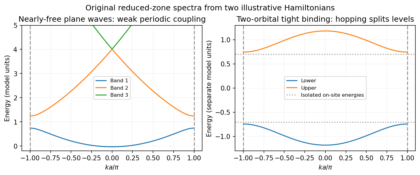


For each orbital degree of freedom per primitive cell there is one band per spin; band filling and the presence of a gap at the Fermi level determine metallic or insulating behavior. The nearly-free limit emphasizes weak Bragg scattering of extended states, while tight binding emphasizes hopping between localized states. They are complementary approximations to electronic band structure, rather than two incompatible explanations of why periodic solids have bands.
Diagonalization and conventions. The spin-dependent part is . For a Hermitian Hamiltonian is real; the supplied lower-band spinor uses the convention , which will be adopted below. The squared spin matrix is . Hence the two ordered energies areIn the plane, let and . ThenIf , use to retain the energy ordering, and interchange the spin directions assigned below. This is an isotropic Rashba effect; has units of inverse length, whereas has units of energy times length.
Band minima. Define and . Completing the square givesAlong , the radial coordinate is , so the lower branch has two minima:In the full plane these are points on a circle of minima . Both branches meet at , . Their ordered energy curves contain : the lower curve descends from the crossing on either side, while the upper rises. Treating them as globally labeled smooth spin branches without switching labels across would obscure the lower-band minima.
Occupied regions and Fermi contours. At zero temperature each spin-split eigenstate with energy below is occupied. PutFor , . The lower-band roots are and , while the upper band is entirely empty. Thus the central disk is unoccupied, the annulus is singly occupied, and the exterior is unoccupied. Both Fermi circles belong to the lower band; there is no doubly occupied region.
At , the lower band is occupied for , giving a singly occupied disk with outer Fermi circle at . The two bands also meet the Fermi energy at the origin. That isolated degenerate point is not a finite doubly occupied disk, and occupation exactly at the Fermi energy is a boundary convention of zero area. Outside the outer circle the states are empty.
For , . The lower branch has outer radius , while the upper branch has inner radius . The disk is doubly occupied, with one state in each band at every momentum. The annulus is singly occupied, in the lower band only, and the exterior is unoccupied. These are the Fermi contours of an isotropic Rashba band; double occupancy here refers to two orthogonal spinor states at the same momentum, not two Electrons occupying one identical quantum state.
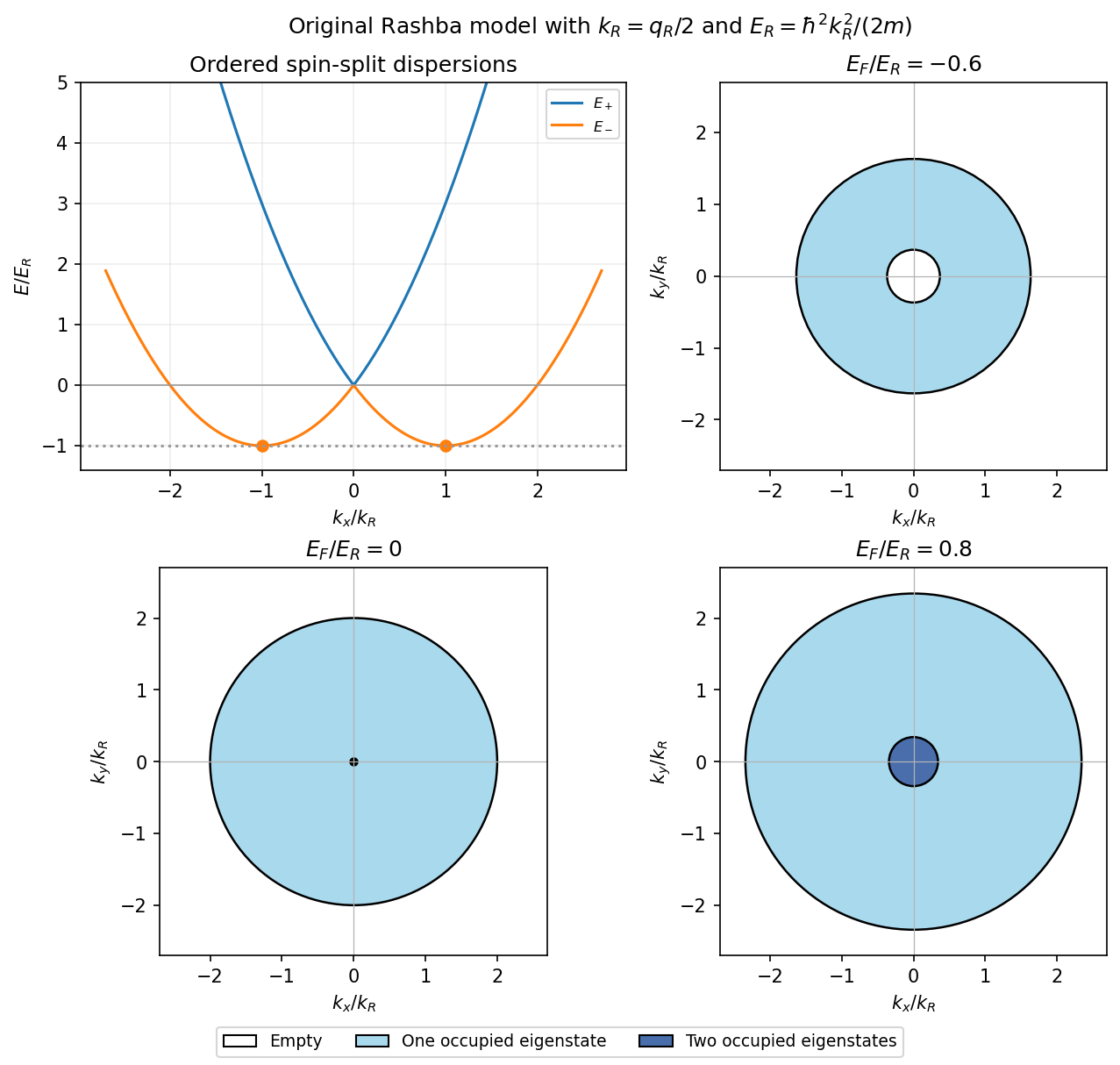
Rashba dispersion and occupied momentum regions below, at and above the band crossing
. Details. 
Inferring the splitting. Above the crossing, the two positive radii differ by :The minimum radius is therefore . It is the difference of the measured radii that is required for ; below the crossing the two lower-band radii instead add to .
Spinors and spin direction. Write , which has for . An orthogonal normalized partner to the supplied lower-band state isIndeed . Direct multiplication by the spin matrix gives eigenvalues and for and , respectively, so orthogonality has selected the other band rather than merely another arbitrary spin basis.
For a normalized spinor , the Pauli expectation values are . Consequently the Rashba spin texture isThe spin lies in the plane and is perpendicular to momentum. On the outer circle , which belongs to , it points clockwise as viewed from ; at it points along . On the inner circle , belonging to , it points counterclockwise; at it points along . Opposite momenta have opposite spins, consistent with time-reversal symmetry. At the origin the eigenstates are degenerate and no unique spin orientation is defined.
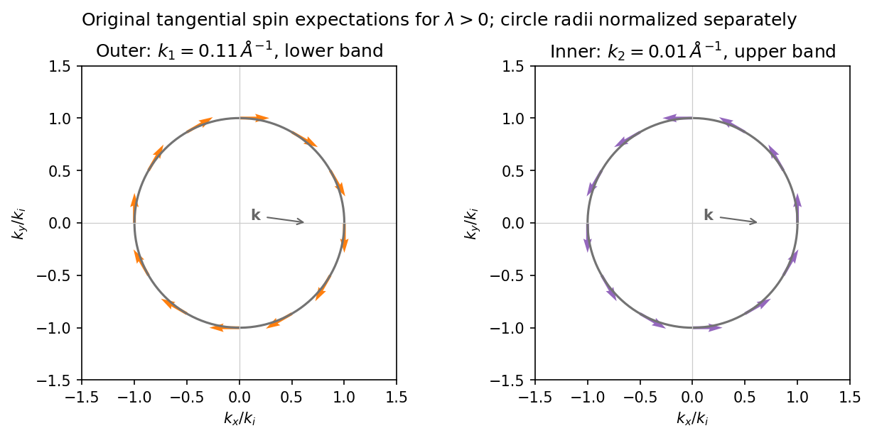
Opposite tangential spin textures on the outer lower-band and inner upper-band Fermi circles
. Details. 
Nondegenerate carrier product. Assume three-dimensional parabolic energy bands near their extrema, spin degeneracy two, and no additional uncounted valley multiplicity. Near the conduction edge, a Boltzmann approximation to the Fermi-Dirac distribution givesAngular integration and the Gaussian radial integral yieldFor valence electron holes, the empty-state probability is . Measuring electron hole kinetic energy downwards from similarly givesThe factors two count spin once in each band. Multiplying cancels the chemical potential and proves the semiconductor mass-action law:In an intrinsic neutral semiconductor, . In a doped equilibrium semiconductor the same product holds under the stated nondegenerate assumptions, even when . Extra valleys or several valence branches must be included in the effective density-of-states factors rather than counted inconsistently.
Equilibrium junction. Put the p region on the left and the n region on the right. Before contact their majority carriers are electron holes and Electrons, respectively. Diffusion initially sends Electrons from n to p and electron holes from p to n. This leaves negative ionized acceptors on the p side and positive ionized donors on the n side, creating a depletion region and an electric field directed from n to p. At equilibrium this field balances diffusion, so the net electric current vanishes.
For a homojunction the gap remains constant while the conduction band and valence band edges bend downwards from p to n by . The equilibrium chemical potential is flat. Since , the electrostatic potential rises from p to n. The carrier profiles satisfyWith fully ionized nondegenerate dopants, the neutral p side has , , while the neutral n side has , . Thus the Electron concentration rises across the junction and the electron hole concentration falls, with both small relative to the far-side majority densities in much of the depleted region. The ideal depletion approximation neglects these mobile populations when calculating the fixed space electric charge, but the actual equilibrium profiles are smooth.
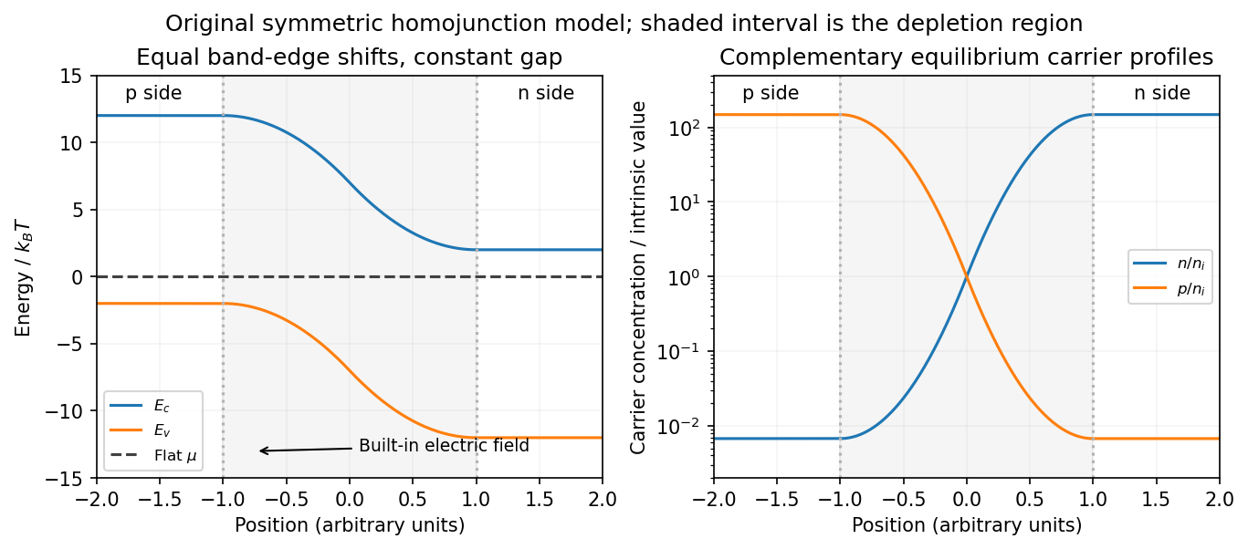
Equilibrium band bending, a flat chemical potential and complementary electron/hole profiles across a homojunction
. Details. 
The built-in potential follows from these Boltzmann factors:There is no applied terminal bias; the internal electrostatic potential variation does not contradict a constant electrochemical potential.
Opposing carrier fluxes under reverse bias. Use for the magnitude of reverse bias and for reverse electric current, as in the PDF. The junction barrier increases by . The Shockley diode equation in that orientation can be writtenThe reverse-directed contribution is supplied by minority Electrons on the p side and minority electron holes on the n side. They reach the depletion edge by diffusion and are swept across by the built-in field. The opposing contribution is associated with majority carriers thermally crossing the barrier in the forward direction; reverse bias suppresses it by the Boltzmann factor. At zero bias detailed balance makes the two equal, while at large enough reverse bias the opposing flux becomes negligible.
In the ideal neutral-region diffusion model,Here are minority-carrier diffusion coefficients, their diffusion lengths, and is junction area. The two terms inside this positive prefactor are the Electron and electron hole contributions; both flow in the same reverse-current direction. This separates the two carrier-species contributions from the two opposing fluxes in the Shockley diode equation. Calling the saturation term a drift current refers to its passage across the depleted region, and does not eliminate the minority-carrier diffusion needed to supply it.
Reading the measured curves. At , the ideal equation gives , initially proportional to reverse electric potential difference. At , it approaches a plateau . The thermal electric potential differences at the three temperatures are about –, consistent with a rise at small reverse biases and near saturation at larger ones. Higher temperature produces a much larger plateau because thermal electron-hole excitation raises exponentially.
The lower-temperature curve has a noticeable residual electric potential difference dependence rather than a perfectly flat plateau. Depletion-region generation, surface leakage or other departures from the ideal diffusion model can contribute. The sharp upturn at the largest reverse electric potential differences is reverse breakdown, outside the unextended Shockley diode equation; the plot alone does not identify a unique microscopic breakdown mechanism. The original horizontal axis duplicates the final decade label, so a precise breakdown electric potential difference cannot be read reliably. Neither issue prevents estimating the gap from the intermediate-bias saturation region.
Band-gap estimate. Use plateau electric currents at a common intermediate reverse bias, away from both the small-bias rise and the breakdown upturn. Approximate readings are , –, and . Kelvin temperatures are required in the activation law.
For fixed effective masses, . If the remaining transport prefactor is approximately constant, extracting a semiconductor band gap from diode saturation current therefore usesUsing the widest temperature separation and the rounded readings givesNeglecting all algebraic prefactors and fitting instead gives about . These differ by roughly , a material correction on the graph's precision scale. Thus an honest graph-based conclusion isThe nonflat low-temperature plateau, rough electric current readings, unprovided temperature dependence of , and possible gap variation prevent a more precise extraction. If depletion-region generation dominated rather than the specified mechanism, its activation slope could involve a different energy scale; the displayed estimate explicitly uses the diffusion-dominated saturation model requested here.
Articles by others on the same topic
There are currently no matching articles.