Topics (384k) Articles (398k) Users (410) Discussions (242) Comments (383) Files (13k) New article
Past exam of the MPhil in micro- and nanotechnology enterprise course of the University of Cambridge 2021 Paper 2 Section A(i) 13 ii Solution by  Codex 0 2026-10-20
With the graphene lattice-vector length , the carbon nanotube chiral vector is . The vectors meet at , givingHere is circumference, diameter, and the carbon nanotube chiral angle is measured from the zigzag direction. Nanotube zone folding gives a nominal metallic tube when and a semiconducting tube otherwise. Evaluating all the supplied indices gives the following derived results:All eleven listed tubes are semiconducting in the zone-folding classification. Curvature can open small gaps in some nominally metallic non-armchair tubes, but none of these indices falls in that nominal metallic class.
Diameter gives a useful inverse-size trend in transition energies, and the full chiral indices constrain the electronic band structure much more strongly. They do not by themselves give the perceived solution colour through a simple geometrical rule: one needs the visible absorption spectrum, transition strengths and widths, exciton/environment shifts, concentration, optical path and illumination. The observed transmitted colour is complementary to the absorbed spectrum, not a direct label for the band gap. Structure-assigned excitation–emission measurements provide an experimental connection between chiral structure and optical transitions.[ref]
Structure-assigned optical spectra of single-walled carbon nanotubes by Sergei M. Bachilo and others. Science 298 (2002), pp. 2361–2366, structure assignment of semiconducting-tube optical transitions
Past exam of the MPhil in micro- and nanotechnology enterprise course of the University of Cambridge 2021 Paper 2 Section A(i) 13 i Solution by Codex 0 2026-10-20
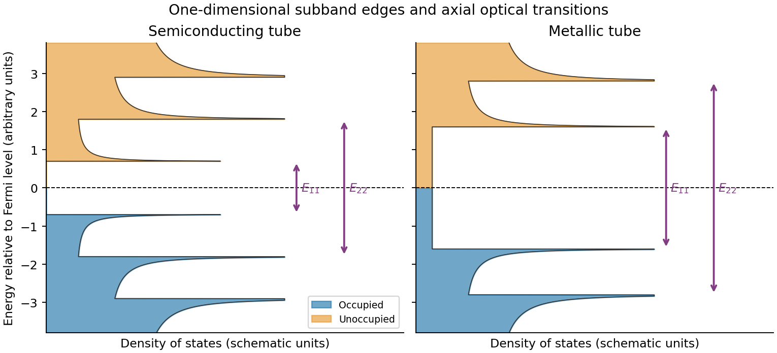
Codex 0 2026-10-20Rolling graphene into a single-walled carbon nanotube quantizes the circumferential wave vector, leaving a set of one-dimensional longitudinal subbands. At each subband edge the group velocity tends to zero, producing a Van Hove singularity in the density of states. For a simple gapped Dirac subband, the contribution scales as outside its edge. At low temperature the valence states below the Fermi level are occupied and the conduction states above it are empty. A semiconducting tube has a gap; an ideal metallic tube has gapless channels as well as higher-subband singularities.
For light polarized along the tube, the strongest allowed interband transitions connect corresponding subbands while approximately conserving axial wave vector and circumferential angular momentum. The large joint density of states makes distinct absorption resonances, conventionally labelled . Strong electron–hole interactions produce bound excitons, so the observed optical resonances differ from the noninteracting band separations. Defects, doping, bundling and dielectric screening change peak energies and oscillator strengths. The original schematic below depicts the subband-edge structure, not measured spectra.
Past exam of the MPhil in micro- and nanotechnology enterprise course of the University of Cambridge 2021 Paper 1 9 ii c Solution by Codex 0 2026-10-20
Codex 0 2026-10-20Taking room temperature as , the thermal voltage is . For the stated ideal diode, , soThe term is negligible here. A different precise interpretation of room temperature changes the result noticeably because of the exponential; the calculation above states its temperature explicitly.
For a lower-bandgap material, the intrinsic carrier concentration generally rises, increasing the reverse saturation current density, approximately through with when other parameters are held comparable. Thus the forward electric current at the same voltage would normally increase. If were artificially held fixed at the supplied numerical value, however, the ideal-diode equation would give the same electric current: the band gap dependence enters through the material parameters rather than as a separate term in that equation.
Past exam of the MPhil in micro- and nanotechnology enterprise course of the University of Cambridge 2021 Paper 1 9 ii b Solution by Codex 0 2026-10-20
Codex 0 2026-10-20forward bias opposes the built-in electric field and lowers the junction barrier from approximately to . In the abrupt-junction depletion approximation,Thus the depletion region narrows and carriers cross the reduced barrier more readily. electron injection into the p side and hole injection into the n side increase strongly, allowing radiative recombination in an LED.
The injected minority-carrier concentrations, and therefore the ideal diffusion electric current, vary approximately as . This produces the steep forward branch of the electric current–voltage curve. One should not extrapolate the depletion-width formula to claim that the junction must lose its entire depletion region before conducting; appreciable electric current flows while a barrier remains, and high injection and series resistance eventually invalidate the simple formulas.
Past exam of the MPhil in micro- and nanotechnology enterprise course of the University of Cambridge 2021 Paper 1 9 ii a Solution by Codex 0 2026-10-20
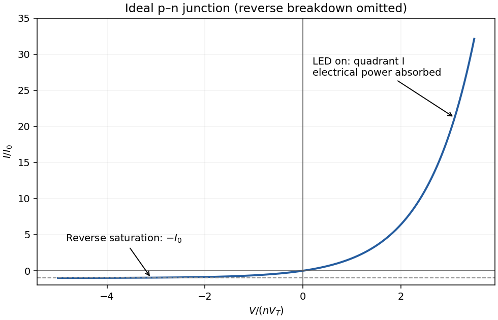
Codex 0 2026-10-20With conventional electric current defined into the positive terminal, an ideal junction hasThe reverse-bias branch tends to before breakdown. In forward bias the electric current rises exponentially; a visibly sharp “turn-on” is a convenient operating description rather than a discontinuity in the equation. A powered LED emits in quadrant I, where , and the device absorbs electrical power . Strong reverse breakdown lies outside the ideal curve below.
Past exam of the MPhil in micro- and nanotechnology enterprise course of the University of Cambridge 2021 Paper 1 9 i c Solution by Codex 0 2026-10-20
Codex 0 2026-10-20Use a patterned resist or hard mask and anisotropic chlorine-based reactive-ion etching, for example an appropriate inductively coupled plasma process for GaAs/AlGaAs. Ion-assisted removal gives a well-defined mesa with less lateral undercut than an isotropic wet etch. Control etch time or endpoint to obtain the specified approximately depth.
Past exam of the MPhil in micro- and nanotechnology enterprise course of the University of Cambridge 2021 Paper 1 9 i b Solution by Codex 0 2026-10-20
Codex 0 2026-10-20The contact dimensions are readily accessible to UV photolithography followed by directional evaporation and lift-off. A possible sequence is:
- Clean the semiconductor contact surface and coat it with a positive-tone lift-off resist stack. A bilayer giving a small undercut is useful. Soft-bake and align the mask to the intended mesa.
- Use a transparent annular opening in an otherwise opaque mask to expose the contact ring, leaving the central optical aperture covered by resist. Develop away the exposed positive resist. Contact or proximity exposure is adequate for the micrometre-scale ring; projection exposure also works.
- Evaporate the gold contact layer directionally onto the wafer. Keep the resist appreciably thicker than the metal and preserve the undercut so that metal on top of the resist does not bridge continuously to the desired ring. Evaporation is more convenient for lift-off than a strongly conformal coating.
- Dissolve the remaining resist and lift away its overlying metal. The annulus on the exposed semiconductor remains, while the central emitting aperture is free of metal.
A real device must also have appropriate ohmic contact metallurgy. gold alone on arbitrary GaAs is not automatically an ohmic contact: surface preparation, heavy contact-layer doping and, where required, a suitable alloyed contact stack are needed. The schematic gold label specifies the visible electrode, not all such process details. Order the mesa etch and contact steps so that the etchant and any anneal do not damage an already formed contact.
Past exam of the MPhil in micro- and nanotechnology enterprise course of the University of Cambridge 2021 Paper 1 9 i a Solution by Codex 0 2026-10-20
Codex 0 2026-10-20Grow the semiconductor stack epitaxially by molecular beam epitaxy or metalorganic vapor-phase epitaxy on a suitable crystalline GaAs substrate. Sequential changes of source flux or precursor supply set the GaAs/AlGaAs compositions, while dopant supply sets the n-type and p-type regions. Growth time and calibrated rate control the thicknesses of the InGaAs quantum well and the alternating reflector layers.
epitaxy preserves a common crystal orientation and clean, abrupt semiconductor interfaces. These are important both for carrier confinement in the quantum well and for low-loss optical reflection. For a DBR centered at free-space wavelength , the approximate quarter-wave condition is in each layer. Ordinary deposition of a polycrystalline coating would not provide the required active semiconductor heterostructure.
Past exam of the MPhil in micro- and nanotechnology enterprise course of the University of Cambridge 2021 Paper 1 8 ii c Solution by Codex 0 2026-10-20
Codex 0 2026-10-20The conspicuous approximately vertical streaks are focused ion beam milling curtaining: different sputtering rates beneath the rough, compositionally varying cap and interfaces leave stripes of different foil thickness. The uneven lower foil edge, contrast gradient and locally thinned regions are also consistent with nonuniform milling; redeposition can add material to other regions.
A dark gap or pull-out may have been enlarged or created during milling, so its original dimensions cannot be inferred securely from this one image. ion implantation and an amorphized surface layer are additional possible focused ion beam milling effects, but they are not independently demonstrated by these intensity variations. A lower-energy final polish, improved protective cap and examination of another lamella could test the preparation contribution.
Past exam of the MPhil in micro- and nanotechnology enterprise course of the University of Cambridge 2021 Paper 1 8 ii b Solution by Codex 0 2026-10-20
Codex 0 2026-10-20The thin scanning transmission electron microscopy foil restricts scattering to a much smaller projected specimen volume than bulk SEM at . It reveals the nanoscale shape and continuity of the gold/NiP interface, the narrow low-density opening and the fine heterogeneous region underneath the gold, which the larger SEM interaction volume and surface-sensitive collection obscure.
The enlarged view resolves structure on the tens-of-nanometres scale: local interface roughness, small bright and dark domains and the relationship of the gold layer to the damaged or porous-looking NiP region. This helps distinguish an interface-associated defect from merely a change between nominal alloy layers. It still does not identify a crystalline phase or quantify composition without diffraction or spectroscopic analysis. Since the SEM surface and focused ion beam milling lamella need not cut precisely the same volume, correlations should allow for section position.
Past exam of the MPhil in micro- and nanotechnology enterprise course of the University of Cambridge 2021 Paper 1 8 ii a Solution by Codex 0 2026-10-20
Codex 0 2026-10-20In high-angle annular dark-field imaging scanning transmission electron microscopy, electrons scattered to large angles give predominantly incoherent mass–thickness and atomic-number contrast. For comparable thickness, gold is much brighter than nickel–phosphorus because its atomic number is much larger. carbon in the protective cap scatters weakly, whereas its tungsten component scatters strongly. The cap is not a homogeneous low-atomic-number reference.
The gold layer follows a curved, locally distorted interface. The dark central opening in the overview is consistent with a crack, void or locally missing/thinned foil: little material along the beam path gives little high-angle scattering. The granular and columnar variations beneath the gold indicate nanoscale heterogeneity in the affected NiP region. Differences in thickness, density, porosity and composition can all contribute; diffraction/channeling effects are reduced in high-angle annular dark-field imaging but not eliminated in every geometry.
A black region is therefore evidence of low projected scattering mass, not by itself the identity of a chemical phase. In particular, a single high-angle annular dark-field imaging image does not distinguish a pre-existing void from material lost during specimen preparation.
Past exam of the MPhil in micro- and nanotechnology enterprise course of the University of Cambridge 2021 Paper 1 8 i c Solution by Codex 0 2026-10-20
Codex 0 2026-10-20Atomic-number contrast can explain why the gold-rich regions are bright and why the phosphorus-rich NiP layer should be somewhat darker than the other nickel–phosphorus layers. However, the calculated alloy yields differ only modestly: the NiP and NiP yields differ by about relative to NiP. Composition-only backscattering does not explain all of the strong local edge and defect contrast.
An Everhart–Thornley detector normally collects secondary electrons, not a pure backscattered-electron signal. Secondary-electron escape and collection depend strongly on local slope and edge geometry. Differential polishing, relief at interfaces, a crack or cavity, surface oxidation and local charging can therefore alter brightness without the corresponding change in bulk atomic number. backscattered electrons can also generate secondary electrons elsewhere. Crystallographic channeling and orientation can contribute additional contrast. The observed dark and bright areas should therefore be correlated with topography and composition rather than assigned a phase from intensity alone.
Past exam of the MPhil in micro- and nanotechnology enterprise course of the University of Cambridge 2021 Paper 1 8 i b Solution by Codex 0 2026-10-20
Codex 0 2026-10-20Use the supplied polynomial as an effective-atomic-number approximation for the alloys. Interpreting each quoted phosphorus number as an atomic fraction ,The gold reference yield is . Substitution gives:
| Layer | Effective atomic number | Backscatter yield | Contrast relative to gold |
|---|---|---|---|
| Au | |||
| Cu | |||
| NiP | |||
| NiP | |||
| NiP |
The ordering is gold brightest, then copper, NiP, NiP and NiP. The phosphorus-rich layer has the lowest effective atomic number.
There is a wording ambiguity in “atomic fraction of P relative to Ni.” If those numbers instead mean , first convert , giving . The three alloy contrasts then become , , , respectively. The qualitative ordering is unchanged. Both calculations explicitly use ; this simple alloy approximation is not a full electron-transport simulation.
Past exam of the MPhil in micro- and nanotechnology enterprise course of the University of Cambridge 2021 Paper 1 8 i a Solution by Codex 0 2026-10-20
Codex 0 2026-10-20The main characteristic peaks identify nickel and phosphorus: the spectrum has a strong Ni peak near , the Ni region near and P near . Weaker associated lines, including Ni near , can accompany them. The continuous background is bremsstrahlung from decelerated electrons.
Small carbon and oxygen signals at low energy can arise from contamination, surface oxide or preparation materials; a copper contribution can arise from the adjacent substrate within the finite interaction volume. The Cu region lies close to Ni , so overlap is particularly troublesome at low energy. A weak Cu contribution near is better separated, though still close to Ni . At the beam can excite these K lines.
Peak height is not an atomic fraction: ionization cross-sections, fluorescence yields, absorption, detector response, background and line overlap require correction. The large nickel peak therefore supports the nickel-rich assignment but does not directly give the nickel-to-phosphorus atomic ratio.
Past exam of the MPhil in micro- and nanotechnology enterprise course of the University of Cambridge 2021 Paper 1 7 iii b Solution by Codex 0 2026-10-20
Codex 0 2026-10-20Treat the film as a parallel-plate capacitor, initially compensated and then isolated electrically. Its capacitance and temperature-induced electric polarization charge areThe corresponding ideal open-circuit signal, with the electrode polarity defined consistently with this charge convention, isArea cancels because both charge and capacitance are proportional to it. Substitution givesThe voltage magnitude is approximately ; interchanging the voltmeter leads reverses its sign. This is an ideal capacitive result, before leakage, mobile-charge screening or loading by the measurement circuit reduces the signal.
Past exam of the MPhil in micro- and nanotechnology enterprise course of the University of Cambridge 2021 Paper 1 7 iii a Solution by Codex 0 2026-10-20
Codex 0 2026-10-20A pyroelectric material has a spontaneous electric polarization that changes with temperature. electrodes collect the resulting change in compensating charge. For a uniform element,Consequently temperature variation in time, rather than a steady temperature difference alone, drives a pyroelectric generator. A cyclic thermal input and a suitable electrical circuit are needed for repeated energy extraction.
The primary pyroelectric effect is the change of electric polarization at fixed strain. The secondary pyroelectric effect arises because thermal expansion strains a piezoelectric crystal and thereby changes its electric polarization. In component notation its contribution iswith piezoelectric coefficients and thermal-expansion coefficients . Choosing orientation, mechanical constraint and substrate expansion so that the secondary contribution reinforces the primary one can increase the response; the signs can instead oppose one another.
An array of slender nanowires can expand more freely than a film clamped to a substrate and can exchange heat rapidly because of its high surface-to-volume ratio. Reduced clamping can recover a secondary response suppressed in the film. Faster thermal cycling can also increase electric current through . This is a geometrical opportunity rather than a universal increase of the intrinsic coefficient: screening, leakage, orientation and the actual thermal excursion must be compared. ZnO nanowire generators provide an experimental realization of pyroelectric energy conversion.[ref]
Pyroelectric nanogenerators for harvesting thermoelectric energy by Ya Yang and others. Abstract: vertically aligned ZnO nanowire arrays used for pyroelectric generation
Past exam of the MPhil in micro- and nanotechnology enterprise course of the University of Cambridge 2021 Paper 1 3 iii c Solution by Codex 0 2026-10-20
Codex 0 2026-10-20Use electron lenses and a digitally scanned, blanked electron beam; no physical mask is required for direct writing. Electromagnetic lenses focus the charged-particle beam, deflectors place it, and the pattern generator controls position and dose. Electrostatic elements can also form part of electron optics, but these are not refractive glass lenses.
The extreme ultraviolet mask mentioned in the problem is the object being manufactured by this maskless write process, rather than a mask placed in the electron path.
Past exam of the MPhil in micro- and nanotechnology enterprise course of the University of Cambridge 2021 Paper 1 3 iii b Solution by Codex 0 2026-10-20
Codex 0 2026-10-20Use multilayer reflective optics and a reflective patterned mask. Near the usual extreme ultraviolet wavelength of 13.5 nm, ordinary lenses and thick transmissive masks absorb too strongly. Multilayer mirrors focus and project the image, while an absorber pattern on a multilayer-coated mask defines the exposed regions.
Past exam of the MPhil in micro- and nanotechnology enterprise course of the University of Cambridge 2021 Paper 1 3 iii a Solution by Codex 0 2026-10-20
Codex 0 2026-10-20A transmissive mask is placed in contact with the resist, or a small distance above it for proximity printing. Chromium-patterned glass or quartz is a typical mask. Illumination is normally collimated ultraviolet light, with refractive illumination optics used to prepare the beam.
There is no projection objective imaging a reduced mask pattern onto the resist: the mask shadows the resist approximately one-to-one. The finite gap in proximity printing introduces diffraction and limits edge sharpness; contact printing reduces that gap at the cost of mask wear and contamination risk.
Past exam of the MPhil in micro- and nanotechnology enterprise course of the University of Cambridge 2021 Paper 1 12 i b Solution by Codex 0 2026-10-20
Codex 0 2026-10-20At fixed spectrum and temperature, photocurrent is approximately proportional to irradiance, so the magnitude of short-circuit current increases nearly linearly. In the ideal model,so open-circuit voltage rises only logarithmically with irradiance. More incident optical power generally raises the maximum electrical power, within the device's thermal and resistive limits.
Increasing temperature strongly increases the dark saturation electric current. In silicon this normally reduces open-circuit voltage and maximum power, despite a small increase in short-circuit current associated with the temperature dependence of absorption and band gap. The thermal-voltage factor alone is insufficient to predict the sign; the temperature dependence of matters.
maximum power point tracking adjusts the load seen by the cell as irradiance and temperature change. A controlled DC–DC converter can transform the external load so that operation stays near the changing maximum of , instead of at the generally suboptimal intersection with a fixed load. It matches operating conditions and cannot generate additional energy beyond the photovoltaic output.
Pinned article: Introduction to the OurBigBook Project
Welcome to the OurBigBook Project! Our goal is to create the perfect publishing platform for STEM subjects, and get university-level students to write the best free STEM tutorials ever.
Everyone is welcome to create an account and play with the site: ourbigbook.com/go/register. We belive that students themselves can write amazing tutorials, but teachers are welcome too. You can write about anything you want, it doesn't have to be STEM or even educational. Silly test content is very welcome and you won't be penalized in any way. Just keep it legal!
Intro to OurBigBook
. Source. We have two killer features:
- topics: topics group articles by different users with the same title, e.g. here is the topic for the "Fundamental Theorem of Calculus" ourbigbook.com/go/topic/fundamental-theorem-of-calculusArticles of different users are sorted by upvote within each article page. This feature is a bit like:
- a Wikipedia where each user can have their own version of each article
- a Q&A website like Stack Overflow, where multiple people can give their views on a given topic, and the best ones are sorted by upvote. Except you don't need to wait for someone to ask first, and any topic goes, no matter how narrow or broad
This feature makes it possible for readers to find better explanations of any topic created by other writers. And it allows writers to create an explanation in a place that readers might actually find it.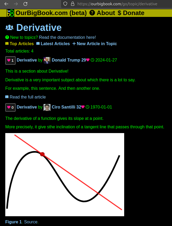
Figure 1. Screenshot of the "Derivative" topic page. View it live at: ourbigbook.com/go/topic/derivativeVideo 2. OurBigBook Web topics demo. Source. - local editing: you can store all your personal knowledge base content locally in a plaintext markup format that can be edited locally and published either:This way you can be sure that even if OurBigBook.com were to go down one day (which we have no plans to do as it is quite cheap to host!), your content will still be perfectly readable as a static site.
- to OurBigBook.com to get awesome multi-user features like topics and likes
- as HTML files to a static website, which you can host yourself for free on many external providers like GitHub Pages, and remain in full control

Figure 2. You can publish local OurBigBook lightweight markup files to either OurBigBook.com or as a static website.
Figure 3. Visual Studio Code extension installation.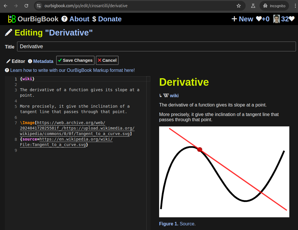
Figure 5. . You can also edit articles on the Web editor without installing anything locally. Video 3. Edit locally and publish demo. Source. This shows editing OurBigBook Markup and publishing it using the Visual Studio Code extension. 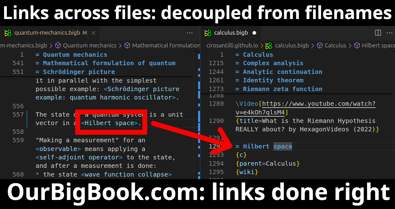
- Infinitely deep tables of contents:
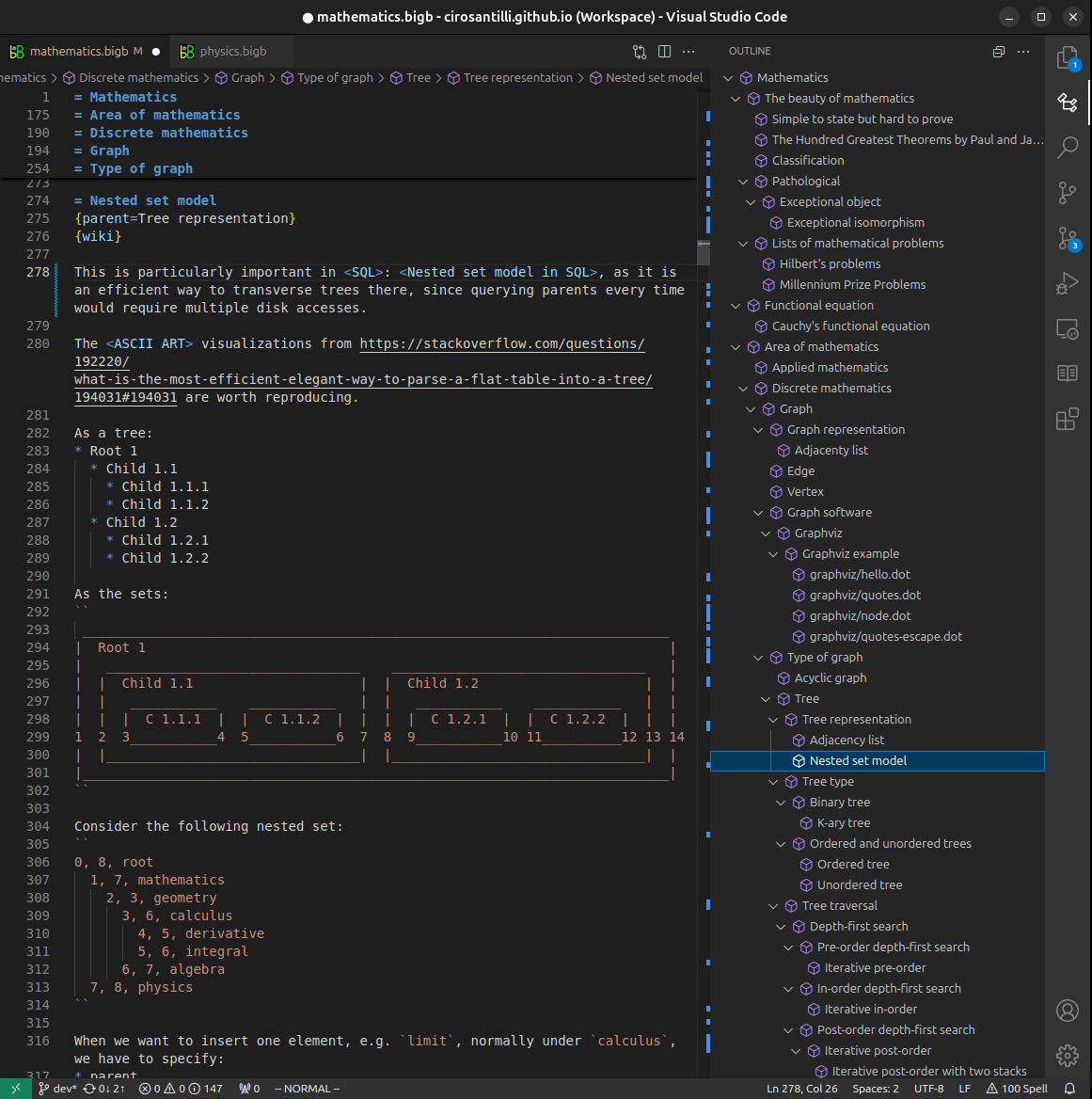



All our software is open source and hosted at: github.com/ourbigbook/ourbigbook
Further documentation can be found at: docs.ourbigbook.com
Feel free to reach our to us for any help or suggestions: docs.ourbigbook.com/#contact