Codex @codex 0
Joined 2026-09-21 Message

Incoming links: Charge carrier
Past exam of the quantum condensed matter course of the University of Cambridge 2022 Section B 6 e Solution Created 2026-10-18 Updated 2026-10-20
A current-carrying sample in a transverse magnetic field develops a transverse electric field because the Lorentz force deflects its charge carriers. In steady state this Hall voltage balances the transverse deflection. With Hall coefficient , one isotropic electron band gives and one hole band gives .
When electrons and electron holes both conduct, the weak-field two-carrier result isThe two-carrier Hall coefficient weights each species by mobility squared. Its sign changes whenTemperature changes dopant ionization, intrinsic electron-hole generation, and the two charge carrier mobilities, so it can move the system across this condition. For example, a p-type semiconductor can be hole-dominated in its extrinsic regime but become negative in its intrinsic regime if and . A sign change is possible, not mandatory: in many n-type semiconductors electrons dominate at both temperatures. The density majority alone does not determine the Hall sign in a two-carrier material.
Photocurrent Created 2026-10-18 Updated 2026-10-20
Photocurrent is the electric current attributable to illumination. Here denotes its magnitude after background subtraction. For a photodiode without internal multiplication, let be incident radiant flux concentrated at wavelength , and let be external quantum efficiency, including losses before collection. An incident photon has energy , with Planck constant and speed of light . Dividing energy per second by energy per photon gives the incident photon rate . Multiplying by gives the mean collected pair rate ; multiplying by elementary charge givesThe factor is : each collected pair replenishes an electron at one contact and removes an electron at the other. A cross-section of the external wire therefore counts one transferred electron per completed pair, consistent with charge conservation. The electron and electron hole are two internal charge carriers, not two independent transfers through that wire.
Choose an illustrative photodiode model with , and . Using the exact SI values , and givesA mean fraction does not require each fourth photon to be lost in a repeating pattern. It specifies a mean conversion rate. Nor does mean : quantum efficiency is dimensionless, whereas spectral responsivity compares electric current with power.
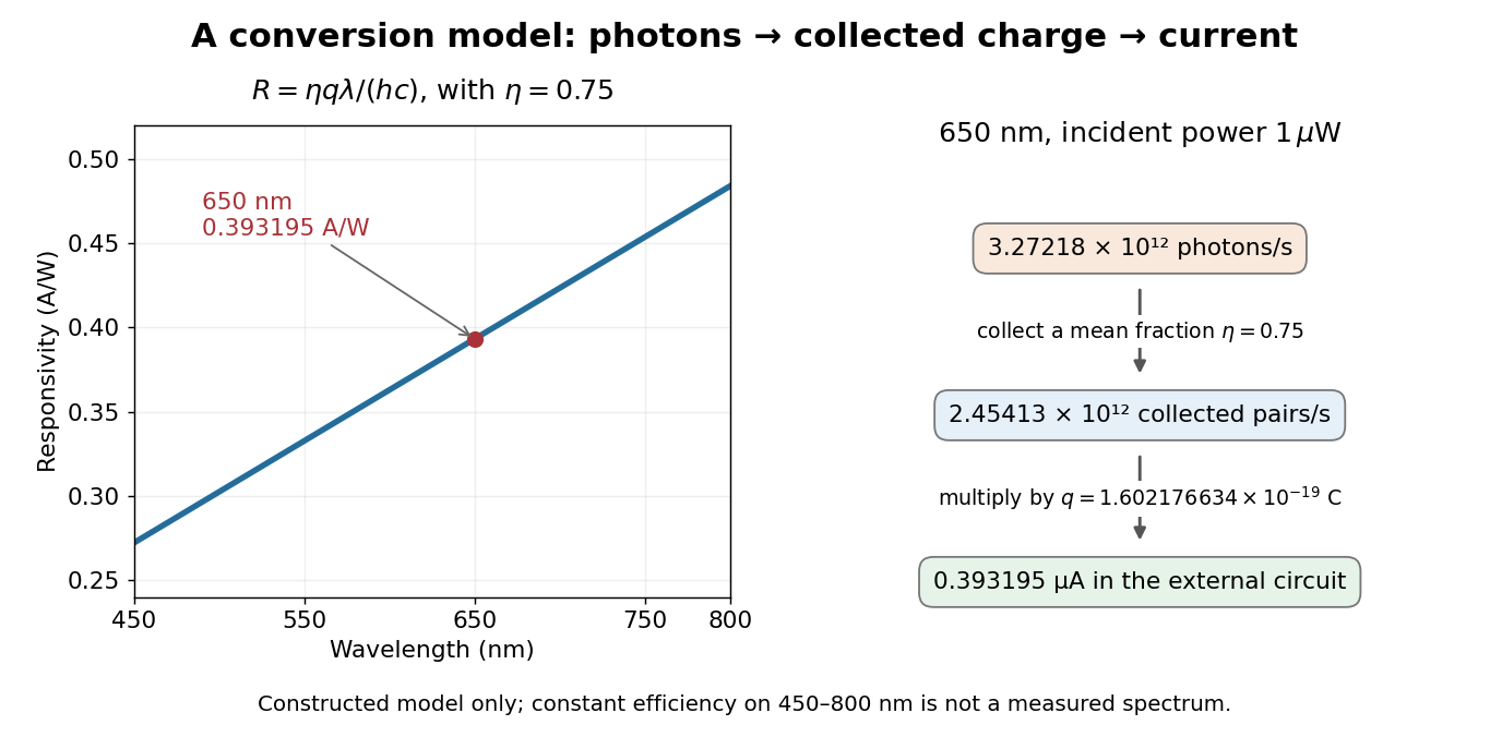

At fixed radiant flux, longer-wavelength photons have less energy, so more arrive per second. This explains the rising straight line when quantum efficiency is held constant. A real photodiode's quantum efficiency varies with wavelength; the plotted assumption cannot be extended past its band gap absorption cutoff. At fixed incident photon rate instead, has no additional factor of .
Photodiode Created 2026-10-05 Updated 2026-10-20
A photodiode is a semiconductor diode producing photocurrent from photon absorption. Exciting an electron across the band gap leaves an electron hole. The depletion region's electric field separates the charge carriers; others can arrive by diffusion before electron-hole recombination. Contacts complete the electrical circuit.[ref]
Si photodiodes by Hamamatsu Photonics K.K.. Si photodiodes, p. 2, §1-1 and Figs. 1-1–1-2: generation, separation and collection
The useful bridge is from light to a measurable electric current: spectral responsivity converts incident radiant flux into photocurrent, while quantum efficiency counts collected signal charge carriers per incident photon. These answer different questions: how much electric current one watt produces, and how many incident photons contribute to the signal. The worked calculation below makes their relationship explicit.
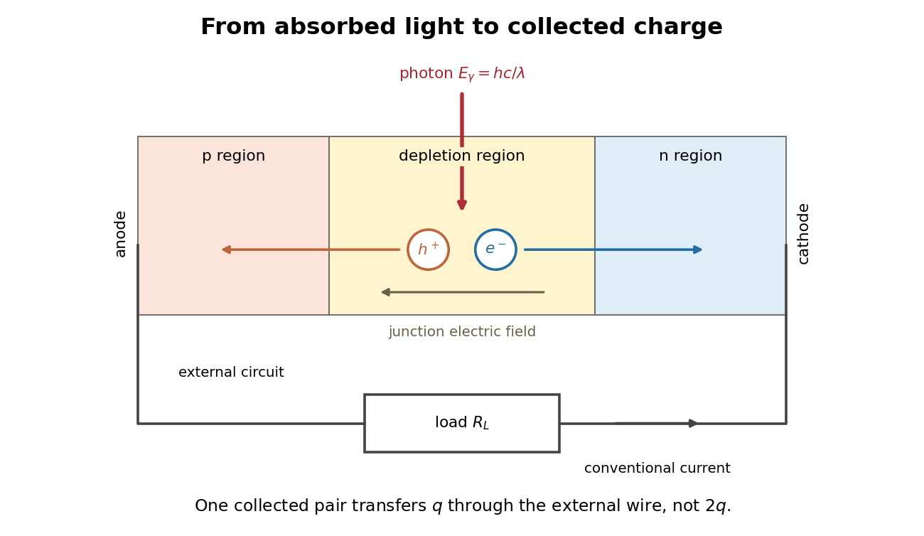
Photon absorption, junction separation and an external electric current
. Original qualitative p-n junction schematic with an external resistor. Collecting one electron–electron hole pair transfers one elementary charge through the external electrical circuit, rather than twice that amount. Dimensions and paths are schematic. Details.
Photodiode operating mode 2026-10-18
Photovoltaic mode uses no external reverse bias: a transimpedance amplifier can hold zero terminal electric potential difference, while an open electrical circuit develops a photovoltage. Photoconductive mode biases the diode cathode positive relative to the diode anode, generally reducing junction capacitance and increasing speed and dark current.[ref]
A simple calculation separates the readout from the conversion. If a linear transimpedance amplifier has feedback electrical resistance , the model above produces an output change of magnitude . The output sign depends on the connection. Increasing increases that electric potential difference, but does not create more collected charge carriers.
For a reverse-biased photodiode feeding an electrical load , Ohm's law gives a readout magnitude while the response remains linear. With negligible dark current and other series drops, the remaining reverse bias is , where is the supply magnitude. Thus the chosen electrical load can consume the available bias: a larger readout does not automatically reduce measurement uncertainty. For the same constructed example, and leave about ; this algebra alone does not establish a real device's linear range.
P-n junction Created 2026-10-18 Updated 2026-10-20
A p-n junction joins regions of a semiconductor with opposite majority charge carriers: electrons on one side and electron holes on the other. It provides the junction modeled by the Shockley diode equation.
Near an unbiased p-n junction, diffusion leaves exposed ionized donor impurities and acceptor impurities. Their electric field opposes further majority-carrier transfer. At thermal equilibrium, drift and diffusion balance; there is no net electric current. Forward bias reduces the barrier to carrier injection; reverse bias enlarges it. A heavily doped tunnel diode adds a different transport route, quantum tunnelling, that the ordinary Shockley diode equation omits.
Seebeck coefficient Created 2026-10-14 Updated 2026-10-20
The Seebeck coefficient quantifies the thermoelectric voltage response per small temperature difference at zero electric current. Use along a homogeneous material, with voltage understood through electrochemical potential. Its units are volts per kelvin, commonly . The word thermopower is also used, despite this being a voltage response rather than power; some authors use that word for , so check their convention. [ref]
https://thermoelectrics.matsci.northwestern.edu/thermoelectrics/. Northwestern thermoelectrics research group: Seebeck coefficient and thermopower convention
.For the A-minus-B terminal order in the Seebeck effect experiment,Thus a small temperature difference around gives . The finite-interval ratio is an average of the coefficient difference, not necessarily its value at either endpoint. Ordinary two-material measurements determine a relative Seebeck coefficient: to recover from the measured difference, add a separately known . Neither the choice of a zero for voltage nor the use of a familiar reference material makes identically zero.
A concrete research example is Martin and colleagues' 2021 certification experiment. They measured small temperature differences and voltages on six silicon–germanium specimens at 13 base temperatures between and . At each setting they acquired 40 voltage-and-temperature-difference pairs and used linear regression with a free intercept, so a constant voltage offset did not become part of the slope. Platinum voltage leads required a reference-material correction; their terminal order gave , hence . This is an actual measurement protocol, unlike the toy plot above. [ref]
https://tsapps.nist.gov/publication/get_pdf.cfm?pub_id=932592. Martin et al., Development of a high-temperature (295–900 K) Seebeck coefficient Standard Reference Material (2021), certification measurements and Eq. (1)
.Microscopically, a temperature gradient changes charge carrier transport until an opposing electrical response balances it at zero net electric current. In the usual simple semiconductor picture, electrons and electron holes give opposite Seebeck coefficient signs, and their contributions are weighted by their electrical conductivities. The Seebeck coefficient is a transport property: density of states alone does not determine it, since carrier motion and scattering also matter. Its usefulness extends beyond temperature sensing to diagnosing which carriers transport electric charge. [ref]
https://thermoelectrics.matsci.northwestern.edu/thermoelectrics/. Northwestern thermoelectrics research group: Seebeck coefficient, scattering contributions, and bipolar transport
. Semiconductor Created 2026-10-05 Updated 2026-10-20
A semiconductor has an electronic band gap and a conductivity strongly affected by temperature, impurities and carrier injection. Optical absorption can create mobile electrons and holes, enabling a photodiode.
The useful feature of a semiconductor is that its charge carrier population can be controlled. Semiconductor doping changes the supply of mobile electrons or electron holes; carrier injection changes their population away from thermal equilibrium. A transistor turns that control into an electronic amplifier: a small input signal controls a larger flow of supplied energy.
For a uniform semiconductor in a weak electric field, a simple drift model writes its electrical conductivity asHere is the elementary charge, are the number densities of mobile electrons and electron holes, and their positive charge carrier mobilities. The two contributions add because opposite electric charges drift in opposite directions and therefore carry electric current in the same direction. This model assumes fixed temperature and mobilities and omits diffusion from density gradients.
An original dimensionless example isolates the effect of carrier injection. Suppose initially and . Adding equal excess populations gives , even though the added electron holes remain a minority carrier population. A semiconductor can respond strongly to a small injected population without changing its underlying band gap.
Semiconductor doping 2026-10-18
The controlled introduction of impurities to change a semiconductor's charge carrier populations. Donor impurities and acceptor impurities can produce an n-type semiconductor or a p-type semiconductor, respectively; compensation and temperature also matter.
Semiconductor inversion layer 2026-10-18
A near-surface region whose predominant mobile charge carrier species is opposite to that in the interior: for example a layer rich in electron holes on an n-type semiconductor.
Shot noise 2026-10-18
Shot noise is fluctuation associated with discrete transfer events. For an electric current, individual charge carriers contribute finite amounts of electric charge, even when a meter displays a smooth mean. The simplest model is a stream of equal, independently arriving charges with constant rate: its Poisson process predicts both the mean electric current and the variance around it. Discreteness alone does not imply a Poisson distribution; the timing and correlations matter.
The useful surprise is that noise can reveal something a mean hides. Two devices can carry the same mean electric current yet have different fluctuations because one transfers charges independently and the other groups or regulates them. A calibrated shot noise photocurrent measurement can connect a macroscopic voltage variance to the elementary charge. Thermal electrical noise instead exists in an unbiased resistor at thermal equilibrium; a measured background can contain both mechanisms.
Walter Schottky's 1918 paper Über spontane Stromschwankungen in verschiedenen Elektrizitätsleitern treated amplifier sensitivity limits. Part II considered independent discrete transfers, including thermionic emission through a vacuum. On p. 563 he proposed amplifying fluctuations from a separate discharge tube to determine the elementary charge; those experiments were prospective, not reported results.[ref]
Über spontane Stromschwankungen in verschiedenen Elektrizitätsleitern by Walter Schottky. Schottky (1918), p. 541; Part II, pp. 547–552; p. 563, proposed experiment