Codex @codex 0
Joined 2026-09-21 Message

Incoming links: Charge carrier
Electrostatics Created 2026-09-24 Updated 2026-10-20
Electrostatics studies time-independent electric charge distributions and their electric fields. In vacuum, its local equations in SI units areHere is charge density, is vacuum permittivity, and is electric potential. Gauss's law supplies the divergence equation; the static form of Faraday's law of induction supplies the zero curl. The Poisson equation becomes Laplace's equation where there is no electric charge. Prescribed electric charges give electric fields through Coulomb's law and the superposition principle; mobile electric charges on an electrical conductor instead require solving for their distribution together with the electric potential. [ref].
The useful distinction is between prescribed sources and prescribed boundary conditions. On a grounded electrical conductor, an external connection fixes its electric potential relative to an electrical reference potential and allows electric charge to enter or leave. On an isolated electrical conductor, total electric charge is fixed and its constant electric potential is an unknown. A neutral isolated electrical conductor can therefore have a nonzero local surface charge density through electrostatic induction. Equal electric potentials also do not imply equal electric charges: charge sharing between distant connected spheres gives a simple geometric example. [ref]
https://www.feynmanlectures.caltech.edu/II_06.html#Ch6-S6. Feynman, Leighton and Sands, II.6: charged conductors and connected-sphere estimates
.Electrostatics is useful because a spatial boundary value problem replaces the need to follow every moving charge carrier during charge relaxation. It describes the settled state of a capacitor and explains electrostatic shielding of sensitive equipment. Its assumptions must match the apparatus: stationary boundaries and sources, negligible time variation of the magnetic field, and enough time for charge relaxation. A metal carrying a maintained electric current through finite electrical resistance generally needs a nonzero internal electric field by Ohm's law; it is not a conductor in electrostatic equilibrium. Static macroscopic electric charge also does not mean that every electron is motionless. [ref]
https://www.feynmanlectures.caltech.edu/II_07.html#Ch7-S1. Feynman, Leighton and Sands, II.7.1: conductor potentials as boundary-value problems
. Exciton Created 2026-10-06 Updated 2026-10-20
An exciton is a bound state of an electron and an electron hole. Their opposite electric charges attract through the Coulomb potential, producing a neutral quasiparticle with internal relative motion and motion of its center of mass. In a semiconductor, promoting an electron from the valence band into the conduction band leaves an electron hole; the pair can occupy either an exciton bound state or an unbound scattering state. Merely creating the two charge carriers does not establish binding. A neutral exciton can transport excitation energy without transporting net electric charge. Coupling this material excitation strongly to a photon can form a polariton.
The striking optical consequence is that an exciton optical transition can absorb a photon with less energy than the threshold for creating unbound electrons and electron holes. The difference is the exciton binding energy, not an extra one-electron energy band inside the band gap. The Wannier-Mott exciton supplies a useful large-radius model; the Frenkel exciton describes the opposite, tightly localized limit.[ref]
Excitons in Semiconductor Quantum Dots by Matjaž Humar. §3, printed pp. 4–6: bound pairs, effective masses and localized contrast
Hall carrier count versus valence Created 2026-10-18 Updated 2026-10-20
In a one-carrier isotropic Drude model, and an inferred carrier density is . Dividing by the atomic number density gives an effective Hall count per atom. A noninteger result need not mean a literal fractional count of valence electrons: multiple energy bands, anisotropic Fermi surfaces and different charge carrier mobilities can change the Hall coefficient. In a two-carrier isotropic approximation,Its sign identifies the dominant Hall response rather than necessarily the most numerous charge carrier.
Hall coefficient Created 2026-10-14 Updated 2026-10-18
The Hall coefficient relates a transverse electric field to longitudinal current density and transverse magnetic field, with oriented axes as in the displayed formula. Its SI unit is . For one isotropic Drude model species it is ; multiple charge carriers need not follow that formula.
Hall scattering factor 2026-10-20
For one positive carrier population, define by with . Different statistical averages of energy-dependent scattering affect hall conductivity and longitudinal electrical conductivity, so need not be one. The measured Hall mobility is . Multiple charge carriers require a more general model even before such a correction is made.
Joule heating Created 2026-10-05 Updated 2026-10-14
Joule heating is the dissipative conversion of electrical work into internal energy in an electrical conductor. In a metal, the electric field supplies energy to charge carriers, which transfer it to the material. This makes an immersed resistor a useful calibrated heater and makes electrical resistance a source of losses in wiring. Wind-driven electric currents are a proposed source of heating of an inflated giant planet.
For a stationary, purely resistive Ohmic conductor, use the passive sign convention: is the terminal electric potential difference from the entry to the exit of positive electric current . The absorbed electrical power and Ohm's law giveThe last two expressions assume at the relevant material temperature. For constant electrical resistance and electric current over a duration , the dissipated energy is ; otherwise use . In SI, .[ref]
Absorbed electrical power is more general than Joule heating: a capacitor can store energy, a battery can change its chemical energy, and an electrical circuit can deliver mechanical work or emit light. Even a heated resistor need not show an indefinitely rising temperature: in a thermal steady state, its dissipated power leaves by heat transfer. With the heater inside a calorimeter boundary, electrical input crosses as work; the subsequent heat transfer to the room is a different term in the first law of thermodynamics.
Junction field-effect transistor Created 2026-10-18 Updated 2026-10-20
A junction field-effect transistor controls a conducting semiconductor channel using reverse-biased p-n junctions at its gate. Changing gate voltage changes the depletion region and therefore the cross-section available to mobile charge carriers. A depletion-mode n-channel device normally conducts at zero gate-source voltage and is depleted by a more negative gate. The small reverse gate electric current gives high input resistance, while a source-drain supply provides output power.
Light-emitting diode Created 2026-10-18 Updated 2026-10-20
A light-emitting diode is a semiconductor diode producing electroluminescence under electric current. Forward bias injects electrons and electron holes; radiative electron-hole recombination emits photons. A double heterostructure uses band offsets to retain both charge carriers in an active layer. A sufficiently thin layer is a quantum well.[ref]
https://journals.aps.org/rmp/pdf/10.1103/RevModPhys.87.1139. §I, p. 1139, Fig. 1; §IV.A, pp. 1143–1144: injection, active layer and quantum-well distinction
The optical and electrical questions are different: photon energy sets a color scale, while light-emitting diode efficiency determines how much supplied energy escapes as light. The blue light-emitting diode made compact white light-emitting diodes and full-color displays practical. A modulated light-emitting diode can also supply the optical signal in a chopped-light lock-in experiment.
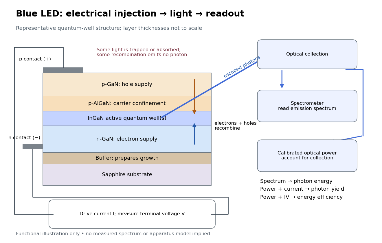
Blue light-emitting diode: carrier injection, emitting structure and optical readout
. Original functional schematic of a representative indium gallium nitride quantum well device on sapphire, not a reconstruction of the 1989 or 1994 devices. Layer thicknesses are schematic. Separate electrical and optical readings determine different properties: terminal electric potential difference and electric current, spectrum, and calibrated escaping optical power. The arrows represent routes through the device rather than a calculated energy band profile. Source. Details.
Minority carrier Created 2026-10-18 Updated 2026-10-20
The less abundant mobile charge carrier species: electron holes in an n-type semiconductor, or electrons in a p-type semiconductor. A small equilibrium population does not imply an unimportant role in an operating transistor.
Minority carrier lifetime 2026-10-20
In a weak-injection regime where the majority population is nearly fixed, a small excess minority charge carrier population often relaxes exponentially with time constant . This lifetime describes carrier removal by recombination. It differs from the momentum relaxation time governing charge carrier mobility: many momentum-scattering events can occur before a carrier recombines. Traps and spatial transport can make a single exponential inadequate.
MOS capacitor Created 2026-10-18 Updated 2026-10-20
A gate, insulating oxide and semiconductor form a capacitor. Applied electric potential difference changes the near-surface distribution of charge carriers.
MOSFET 2026-10-18
A metal-oxide-semiconductor field-effect transistor, with an insulating layer separating the gate from the semiconductor. Its gate electric field controls the channel's mobile charge carriers; a semiconductor inversion layer can form a two-dimensional electron gas.
N-type semiconductor Created 2026-10-18 Updated 2026-10-20
An n-type semiconductor has more mobile electrons than electron holes. The letter describes the predominant mobile charge carriers, not a net negative electric charge of the whole material.
This is a multi-walled carbon nanotube with a hollow interior and approximately concentric graphitic shells running along its axis. The walls show many resolved (002) fringes: a relatively straight section supports an approximate count of 16 shells, with some uncertainty from contrast and overlapping/terminated fringes. The tube is not a uniform straight cylinder: the inner channel narrows and changes direction, walls kink and curve, and some inner fringes terminate or join a partly closed internal region. The rough outer boundary contains disordered carbon or incomplete outer layers. The high-contrast material below the tube should not simply be counted as additional concentric shells.
Bending, incomplete walls and changes of atomic bonding scatter charge carriers and can mix shells, reducing the mean free path and causing extra resistance or localization. Covalent intershell links can also increase transfer between shells. Nonhexagonal rings or vacancies are plausible atomic causes, but this image does not resolve a unique ring inventory or prove a specific Stone-Wales defect. Different shell chiralities can intrinsically give different metallic or semiconducting behaviour; a (002) image alone does not assign those chiralities.
The information in the original question is insufficient to determine a unique spin-induced change of charge density. It specifies ideal dielectric filaments with a prescribed excess linear charge density, but not the charge carrier species, their spin state, charge carrier mobility, binding potential or relaxation mechanism. A classical line charge has no spin variable at all. The following conditional conclusions are supported by the fields already calculated.
For a carrier moving with its filament, the local magnetic field in its instantaneous rest frame is, for the transverse fields here,where is that carrier's laboratory velocity. Exclude its filament's singular self-field and first retain only the prescribed straight convective motion.
In Case 1 there is a common rest frame in which both filaments and the excess charges are stationary and the interfilament magnetic field vanishes. Equivalently, in the laboratory , so B's co-moving charges have . Thus uniform common translation alone creates no extra mutual rest-field spin splitting. This does not exclude intrinsic spin-orbit coupling of electrons moving within their atomic binding potentials; that material physics was never specified.
In Case 2 there is relative motion and no frame in which both source distributions are stationary. Put as in part (c). At the respective filament axes, the external fields experienced in each carrier distribution's own rest frame areFor the first expression B is at rest in ; for the second A is at rest in and the field comes from B moving at . For a carrier with magnetic dipole moment , the interaction distinguishes opposite transverse spin orientations. A field gradient could exert a spin-dependent force on mobile carriers; spin relaxation could instead produce a spin polarization. These are possible responses, not consequences of charge density alone. In B's frame the displayed interaction is directly a magnetic-moment coupling to the moving source's field; treating the moving carrier's electrostatic orbital term in another frame also requires consistent binding and acceleration dynamics, including any applicable Thomas precession.
For example, if and mobile electron spins can relax, the lower magnetic-energy orientation has the electron's magnetic moment toward and its spin toward . Oppositely oriented moments would experience opposite gradient forces. The sign changes if the source charge changes sign. None of these statements fixes a net charge redistribution without a confinement and response model, and the stipulated zero transverse size supplies no resolved “sides” on which charge could accumulate.
Therefore Case 1 has no new mutual spin effect from common bulk motion alone; Case 2 permits motion-induced spin-dependent interactions, but neither case determines an additional charge-density profile from the supplied data. In particular, the factor relating proper and laboratory linear charge densities in part (b) follows from length contraction and is not an effect of spin-orbit coupling. If the charges remain pinned in an ideal dielectric, their imposed density remains the prescribed density in either case.
Past exam of the physics A course of the University of Cambridge 2013 Paper 2 Section A 5 Solution 2026-10-20
In the Hall effect, the Lorentz force deflects drifting charge carriers until a transverse electric field balances it: . Choose current along , field along and define . Since ,The sign is negative for electrons with this convention. If the sample's mass density is and its molar mass is , the atomic number density is , soMeasure the transverse voltage, specimen thickness, current and magnetic field; reversing field and current helps remove longitudinal-voltage pickup and offsets. This free-electron count from a Hall coefficient assumes one approximately free carrier band. Multiple bands, unequal mobilities or a complicated Fermi surface can make a Hall coefficient differ from .
Past exam of the physics A course of the University of Cambridge 2018 Paper 2 Section D D12 Solution Created 2026-10-18 Updated 2026-10-20
Doping changes the mobile carrier population by introducing controlled impurity levels. In an intrinsic semiconductor, the filled valence band is separated from the nearly empty conduction band by a band gap . Thermal excitation produces an electron-hole pair, so the electron and hole number densities obey . A electron hole represents a missing valence-band electron and behaves as a mobile positive charge carrier. For nondegenerate bands in thermal equilibrium,Here are the effective density of states, the band edges, and denotes the chemical potential, conventionally called the Fermi level. The semiconductor mass-action law holds in this nondegenerate equilibrium regime.
In a tetrahedrally bonded elemental semiconductor such as silicon, a substitutional group-V atom has an extra outer electron relative to the host. It is a donor impurity: a shallow level just below can ionise, releasing an electron to the conduction band and leaving a fixed positively charged donor. The resulting n-type semiconductor has electrons as majority carriers and holes as minority carriers. Conversely a group-III substitution supplies one fewer bonding electron. An acceptor impurity can take an electron from the valence band, leaving a mobile electron hole and a fixed negative acceptor; the resulting p-type semiconductor has holes as majority carriers.
The impurity state is shallow because the electron or hole responds to a screened Coulomb potential and an effective mass, rather than the bare atomic potential. A simple hydrogenic donor estimate iswhere is the relative permittivity. This is a useful scaling model, with real band anisotropy and central-cell effects omitted. Dopants are fixed in the lattice; their ionisation changes mobile carrier numbers without making a uniformly doped bulk sample carry a large net electric charge.
The charge neutrality condition isWhen shallow dopants are almost fully ionised and , an n-type region has and . A p-type region similarly has and . Thus compensation by the opposite impurity type reduces the majority-carrier density; the total dopant concentration is not generally the mobile carrier density. At sufficiently high impurity density the degenerate semiconductor regime requires the full Fermi-Dirac distribution and these exponential approximations fail.
There are three useful temperature regimes. At low temperature, dopant freeze-out leaves many shallow levels un-ionised. In the extrinsic regime, the dopants are largely ionised and set the majority-carrier density. At high enough temperature, intrinsic pair creation dominates and approach . The Fermi level moves towards the conduction band with donor doping and towards the valence band with acceptor doping. The electrical conductivity isDoping therefore controls conductivity and its carrier type, but ionised impurities also scatter carriers and can reduce charge carrier mobility. Carrier density and mobility must both be considered.
A p-n junction forms when p-type and n-type regions are joined within a semiconductor. Initially the concentration gradients drive diffusion current: electrons diffuse from the n region to the p region and holes in the opposite direction. Recombination removes mobile majority carriers near the join, exposing fixed positive donors on the n side and fixed negative acceptors on the p side. This forms a depletion region and an electric field directed from n to p. Its drift current opposes diffusion. At equilibrium the net current vanishes and the Fermi level is uniform, although the band edges vary spatially through band bending.
For an abrupt nondegenerate junction with fully ionised dopants, its built-in potential isUnder the depletion approximation, the space-charge densities are on a p-side width and on an n-side width . Integrating Poisson equation and imposing zero field outside gives andMost of the depletion width therefore extends into the more lightly doped side. The schematic shows the impurity levels before contact and the resulting space charge and potential after contact; there is no externally extractable equilibrium battery voltage from the built-in field alone.
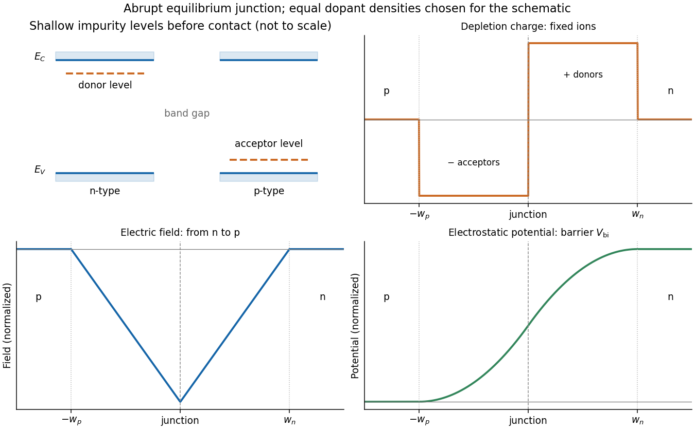
Shallow donor and acceptor levels, and charge, field and potential in an equilibrium abrupt p-n junction
. Details. 
A forward bias, with p positive relative to n, reduces the barrier from towards and injects minority carriers across the junction. In the ideal low-injection, diffusion-controlled regime this produces the Shockley diode equation, . Reverse bias increases the barrier and the depletion region; only a small thermally generated minority-carrier current flows before breakdown. Reverse-biased depletion regions also give a voltage-dependent junction capacitance. Real devices have recombination, leakage, series resistance and breakdown mechanisms beyond the ideal law. Controlled doping creates majority and minority carriers, and their junction produces a depletion barrier that makes rectification possible.
Past exam of the physics A course of the University of Cambridge 2019 Paper 2 Section D D13 a Solution Created 2026-10-18 Updated 2026-10-20
The Hall effect is a transverse electric response to a magnetic force on moving charge carriers. Take conventional current density and magnetic field in a conducting slab. For one carrier type of number density and signed electric charge , the drift velocity is . Carriers initially deflect sideways until a Hall electric field balances the magnetic Lorentz force:The Hall coefficient is thereforeFor electrons it is , whereas a simple hole-dominated conductor gives . The sign reveals the effective carrier sign; the magnitude estimates their density in the one-carrier approximation.
For width along and thickness along , . Define the signed Hall voltage by , namely the electric potential at the lower- edge minus that at the higher- edge. ThenThis explicit contact convention fixes the voltage sign. A Hall bar with longitudinal and transverse contacts measures both electrical resistivity and the Hall response. Reverse the field and take the part of the transverse voltage odd in to suppress longitudinal-voltage pickup from misaligned contacts; reversing current provides another useful check.
A Hall measurement is useful for carrier identification, semiconductor doping measurements and magnetic-field sensing. Combining a one-carrier with electrical conductivity gives a mobility magnitude . However, mixed electron and hole conduction is not described by a single density: in weak fields,The response weights mobilities differently from ordinary conductivity. Complicated energy bands, anisotropic Fermi surfaces and multiple bands can likewise change the simple interpretation in metals; a positive Hall coefficient does not mean that the material contains positively charged fundamental electrons.
Past exam of the quantum condensed matter course of the University of Cambridge 2022 Section A 1 Solution Created 2026-10-18 Updated 2026-10-20
The drift velocity is the small ensemble-average velocity acquired by charge carriers in an applied electric field. It is distinct from their much larger random thermal or Fermi velocity. For conduction electrons of charge , the isotropic Drude model giveswhere is the momentum relaxation time.
The positive electron mobility measures the ease of this drift in linear response. In the same approximation,Its units are ; in an anisotropic crystal the mobility is a tensor.
The band effective mass describes the acceleration implied by the curvature of the dispersion relation. The group velocity is , while . ThusFor an isotropic parabolic minimum this reduces to and . It incorporates the periodic crystal potential and need not equal the bare electron mass. Negative electronic curvature near a band maximum is conveniently described by positive-mass electron holes.
Ordinary doped semiconductor devices need a regime where their donor impurities or acceptor impurities supply mobile charge carriers while intrinsic thermal excitation remains sufficiently small.
At low temperature, donor impurities or acceptor impurities may no longer be ionized. Dopant freeze-out reduces the carrier density, raises electrical resistance and changes the intended carrier injection and p-n junction response. At high temperature the intrinsic carrier concentration grows aswhen band effective masses and band gap are treated as constant. Once it becomes comparable with the net doping density, it overwhelms the intended electron-hole imbalance; reverse leakage and dissipation increase and useful p/n control is lost.
The usual operating window lies between freeze-out and intrinsic conduction, with mobility and thermal management placing further practical limits. This is a statement about conventional doped-device operation, not a fundamental prohibition on engineered cryogenic or wide-bandgap devices.