Born: 1965
Died: 2010+-ish
This is the lowest level of abstraction computer, at which the basic gates and power are described.
At this level, you are basically thinking about the 3D layered structure of a chip, and how to make machines that will allow you to create better, usually smaller, gates.
What a legendary place.
As mentioned at youtu.be/16BzIG0lrEs?t=397 from Video "Applied Materials by Asianometry (2021)", originally the companies fabs would make their own equipment. But eventually things got so complicated that it became worth it for separate companies to focus on equipment, which then then sell to the fabs.
How ASML Won Lithography by Asianometry (2021)
Source. First there were dominant Elmer and Geophysics Corporation of America dominating the market.
Then a Japanese government project managed to make Nikon and Canon Inc. catch up, and in 1989, when Ciro Santilli was born, they had 70% of the market.
youtu.be/SB8qIO6Ti_M?t=240 In 1995, ASML had reached 25% market share. Then it managed the folloging faster than the others:
- TwinScan, reached 50% market share in 2002
- Immersion litography
- EUV. There was a big split between EUV vs particle beams, and ASML bet on EUV and EUV won.
- youtu.be/SB8qIO6Ti_M?t=459 they have an insane number of software engineers working on software for the machine, which is insanely complex. They are big on UML.
- youtu.be/SB8qIO6Ti_M?t=634 they use ZEISS optics, don't develop their own. More precisely, the majority owned subsidiary Carl Zeiss SMT.
- youtu.be/SB8qIO6Ti_M?t=703 IMEC collaborations worked well. Notably the ASML/Philips/ZEISS trinity
- www.youtube.com/watch?v=XLNsYecX_2Q ASML: Chip making goes vacuum with EUV (2009) Self promotional video, some good shots of their buildings.
Parent/predecessor of ASML.
Applied Materials by Asianometry (2021)
Source. They are chemical vapor deposition fanatics basically.This is the mantra of the semiconductor industry:
- power and area are the main limiting factors of chips, i.e., your budget:
- chip area is ultra expensive because there are sporadic errors in the fabrication process, and each error in any part of the chip can potentially break the entire chip. Although there areThe percentage of working chips is called the yield.In some cases however, e.g. if the error only affects single CPU of a multi-core CPU, then they actually deactivate the broken CPU after testing, and sell the worse CPU cheaper with a clear branding of that: this is called binning www.tomshardware.com/uk/reviews/glossary-binning-definition,5892.html
- power is a major semiconductor limit as of 2010's and onwards. If everything turns on at once, the chip would burn. Designs have to account for that.
- performance is the goal.Conceptually, this is basically a set of algorithms that you want your hardware to solve, each one with a respective weight of importance.Serial performance is fundamentally limited by the longest path that electrons have to travel in a given clock cycle.The way to work around it is to create pipelines, splitting up single operations into multiple smaller operations, and storing intermediate results in memories.
They put a lot of expensive equipment together, much of it made by other companies, and they make the entire chip for companies ordering them.
A list of fabs can be seen at: en.wikipedia.org/wiki/List_of_semiconductor_fabrication_plants and basically summarizes all the companies that have fabs.
Some nice insights at: Robert Noyce: The Man Behind the Microchip by Leslie Berlin (2006).
AMD just gave up this risky part of the business amidst the fabless boom. Sound like a wise move. They then fell more and more away from the state of the art, and moved into more niche areas.
SMIC, Explained by Asianometry (2021)
Source. One of the companies that has fabs, which buys machines from companies such as ASML and puts them together in so called "silicon fabs" to make the chips
As the quintessential fabless fab, there is on thing TSMC can never ever do: sell their own design! It must forever remain a fab-only company, that will never compete with its customers. This is highlighted e.g. at youtu.be/TRZqE6H-dww?t=936 from Video "How Nvidia Won Graphics Cards by Asianometry (2021)".
- UCM failed because it focused too much on the internal market, and was shielded from external competition, so it didn't become world leading
- one of TSMC's great advances was the fabless business model approach.
- they managed to do large technology transfers from the West to kickstart things off
- one of their main victories was investing early in CMOS, before it became huge, and winning that market
Basically what register transfer level compiles to in order to achieve a real chip implementation.
After this is done, the final step is place and route.
They can be designed by third parties besides the semiconductor fabrication plants. E.g. Arm Ltd. markets its Artisan Standard Cell Libraries as mentioned e.g. at: web.archive.org/web/20211007050341/https://developer.arm.com/ip-products/physical-ip/logic This came from a 2004 acquisition: www.eetimes.com/arm-to-acquire-artisan-components-for-913-million/, obviously.
The standard cell library is typically composed of a bunch of versions of somewhat simple gates, e.g.:and so on.
Each of those gates has to be designed by hand as a 3D structure that can be produced in a given fab.
Simulations are then carried out, and the electric properties of those structures are characterized in a standard way as a bunch of tables of numbers that specify things like:Those are then used in power, performance and area estimates.
Open source ones:
- www.quora.com/Are-there-good-open-source-standard-cell-libraries-to-learn-IC-synthesis-with-EDA-tools/answer/Ciro-Santilli Are there good open source standard cell libraries to learn IC synthesis with EDA tools?
A set of software programs that compile high level register transfer level languages such as Verilog into something that a fab can actually produce. One is reminded of a compiler toolchain but on a lower level.
The most important steps of that include:
- logic synthesis: mapping the Verilog to a standard cell library
- place and route: mapping the synthesis output into the 2D surface of the chip
Step of electronic design automation that maps the register transfer level input (e.g. Verilog) to a standard cell library.
The output of this step is another Verilog file, but one that exclusively uses interlinked cell library components.
Given a bunch of interlinked standard cell library elements from the logic synthesis step, actually decide where exactly they are going to go on 2D (stacked 2D) integrated circuit surface.
Sample output format of place and route would be GDSII.

The main ones as of 2020 are:
- Mentor Graphics, which was bought by Siemens in 2017
- Cadence Design Systems
- Synopsys
Very good channel to learn some basics of semiconductor device fabrication!
Focuses mostly on the semiconductor industry.
youtu.be/aL_kzMlqgt4?t=661 from Video "SMIC, Explained by Asianometry (2021)" from mentions he is of Chinese ascent, ancestors from Ningbo. Earlier in the same video he mentions he worked on some startups. He doesn't appear to speak perfect Mandarin Chinese anymore though based on pronounciation of Chinese names.
Reflecting on Asianometry in 2022 by Asianometry (2022)
Source. Mentions his insane work schedule: 4 hours research in the morning, then day job, then editing and uploading until midnight. Appears to be based in Taipei. Two videos a week. So even at the current 400k subs, he still can't make a living.It is quite amazing to read through books such as The Supermen: The Story of Seymour Cray by Charles J. Murray (1997), as it makes you notice that earlier CPUs (all before the 70's) were not made with integrated circuits, but rather smaller pieces glued up on PCBs! E.g. the arithmetic logic unit was actually a discrete component at one point.
The reason for this can also be understood quite clearly by reading books such as Robert Noyce: The Man Behind the Microchip by Leslie Berlin (2006). The first integrated circuits were just too small for this. It was initially unimaginable that a CPU would fit in a single chip! Even just having a very small number of components on a chip was already revolutionary and enough to kick-start the industry. Just imagine how much money any level of integration saved in those early days for production, e.g. as opposed to manually soldering point-to-point constructions. Also the reliability, size an weight gains were amazing. In particular for military and spacial applications originally.
Uploaded by the Computer History Museum. There is value in tutorials written by early pioneers of the field, this is pure gold.
Shows:
- photomasks
- silicon ingots and wafer processing
Register transfer level is the abstraction level at which computer chips are mostly designed.
The only two truly relevant RTL languages as of 2020 are: Verilog and VHDL. Everything else compiles to those, because that's all that EDA vendors support.
Much like a C compiler abstracts away the CPU assembly to:
- increase portability across ISAs
- do optimizations that programmers can't feasibly do without going crazy
Compilers for RTL languages such as Verilog and VHDL abstract away the details of the specific semiconductor technology used for those exact same reasons.
Examples of companies that work at this level include:
But once designs started getting very complicated, it started to make sense to separate concerns between designers and fabs.
What this means is that design companies would primarily write register transfer level, then use electronic design automation tools to get a final manufacturable chip, and then send that to the fab.
The term "Fabless" could in theory refer to other areas of industry besides the semiconductor industry, but it is mostly used in that context.
One very good thing about this is that it makes it easy to create test cases directly in C++. You just supply inputs and clock the simulation directly in a C++ loop, then read outputs and assert them with
assert(). And you can inspect variables by printing them or with GDB. This is infinitely more convenient than doing these IO-type tasks in Verilog itself.Some simulation examples under verilog.
First install Verilator. On Ubuntu:Tested on Verilator 4.038, Ubuntu 22.04.
sudo apt install verilatorRun all examples, which have assertions in them:
cd verilator
make run
File structure is for example:
- verilog/counter.v: Verilog file
- verilog/counter.cpp: C++ loop which clocks the design and runs tests with assertions on the outputs
- verilog/counter.params: gcc compilation flags for this example
- verilog/counter_tb.v: Verilog version of the C++ test. Not used by Verilator. Verilator can't actually run out
_tbfiles, because they do in Verilog IO things that we do better from C++ in Verilator, so Verilator didn't bother implementing them. This is a good thing.
Example list:
- verilog/negator.v, verilog/negator.cpp: the simplest non-identity combinatorial circuit!
- verilog/counter.v, verilog/counter.cpp: sequential hello world. Synchronous active high reset with active high enable signal. Adapted from: www.asic-world.com/verilog/first1.html
- verilog/subleq.v, verilog/subleq.cpp: subleq one instruction set computer with separated instruction and data RAMs
The example under verilog/interactive showcases how to create a simple interactive visual Verilog example using Verilator and SDL.
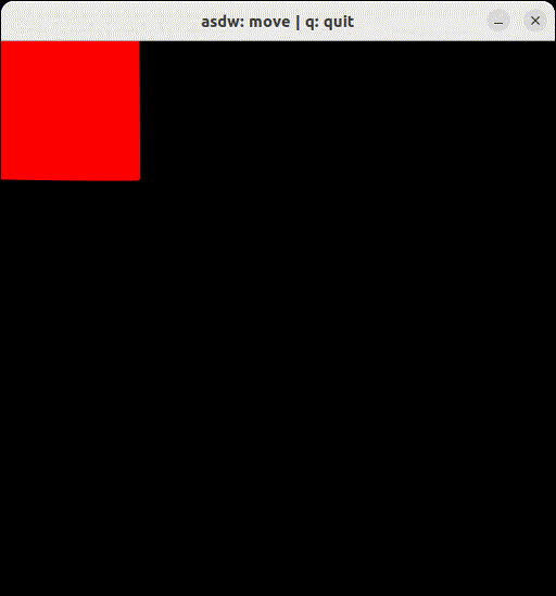
You could e.g. expand such an example to create a simple (or complex) video game for example if you were insane enough. But please don't waste your time doing that, Ciro Santilli begs you.
The example is also described at: stackoverflow.com/questions/38108243/is-it-possible-to-do-interactive-user-input-and-output-simulation-in-vhdl-or-ver/38174654#38174654
Usage: install dependencies:then run as either:Tested on Verilator 4.038, Ubuntu 22.04.
sudo apt install libsdl2-dev verilatormake run RUN=and2
make run RUN=moveFile overview:
In those examples, the more interesting application specific logic is delegated to Verilog (e.g.: move game character on map), while boring timing and display matters can be handled by SDL and C++.
Examples under vhdl.
Run all examples, which have assertions in them:
cd vhdl
./run
Files:
- Examples
- Basic
- vhdl/hello_world_tb.vhdl: hello world
- vhdl/min_tb.vhdl: min
- vhdl/assert_tb.vhdl: assert
- Lexer
- vhdl/comments_tb.vhdl: comments
- vhdl/case_insensitive_tb.vhdl: case insensitive
- vhdl/whitespace_tb.vhdl: whitespace
- vhdl/literals_tb.vhdl: literals
- Flow control
- vhdl/procedure_tb.vhdl: procedure
- vhdl/function_tb.vhdl: function
- vhdl/operators_tb.vhdl: operators
- Types
- vhdl/integer_types_tb.vhdl: integer types
- vhdl/array_tb.vhdl: array
- vhdl/record_tb.vhdl.bak: record. TODO fails with "GHDL Bug occurred" on GHDL 1.0.0
- vhdl/generic_tb.vhdl: generic
- vhdl/package_test_tb.vhdl: Packages
- vhdl/standard_package_tb.vhdl: standard package
- textio
* vhdl/write_tb.vhdl: write
* vhdl/read_tb.vhdl: read - vhdl/std_logic_tb.vhdl: std_logic
- vhdl/stop_delta_tb.vhdl:
--stop-delta
- Basic
- Applications
- Combinatoric
- vhdl/adder.vhdl: adder
- vhdl/sqrt8_tb.vhdl: sqrt8
- Sequential
- vhdl/clock_tb.vhdl: clock
- vhdl/counter.vhdl: counter
- Combinatoric
- Helpers
* vhdl/template_tb.vhdl: template
Some examples:
Ubuntu 25.04 GCC 14.2 -O0 x86_64 produces a horrendous:To do about 1s on P14s we need 2.5 billion instructions:and:gives:
11c8:       48 83 45 f0 01          addq   $0x1,-0x10(%rbp)
11cd:       48 8b 45 f0             mov    -0x10(%rbp),%rax
11d1:       48 3b 45 e8             cmp    -0x18(%rbp),%rax
11d5: 72 f1 jb 11c8 <main+0x7f>time ./inc_loop.out 2500000000time ./inc_loop.out 2500000000 1,052.22 msec task-clock # 0.998 CPUs utilized
23 context-switches # 21.858 /sec
12 cpu-migrations # 11.404 /sec
60 page-faults # 57.022 /sec
10,015,198,766 instructions # 2.08 insn per cycle
# 0.00 stalled cycles per insn
4,803,504,602 cycles # 4.565 GHz
20,705,659 stalled-cycles-frontend # 0.43% frontend cycles idle
2,503,079,267 branches # 2.379 G/sec
396,228 branch-misses # 0.02% of all branchesWith -O3 it manages to fully unroll the loop removing it entirely and producing:to is it smart enough to just return the return value from strtoll directly as is in
    1078:       e8 d3 ff ff ff          call   1050 <strtoll@plt>
}
    107d:       5a                      pop    %rdx
107e: c3 retrax.This is the only way that we've managed to reliably get a single
inc instruction loop, by using inline assembly, e.g. on we do x86:loop:
inc %[i];
cmp %[max], %[i];
jb loop;For 1s on P14s Ubuntu 25.04 GCC 14.2 -O0 x86_64 we need about 5 billion:
time ./inc_loop_asm.out 5000000000This is a quick Microarchitectural benchmark to try and determine how many functional units our CPU has that can do an
inc instruction at the same time due to superscalar architecture.The generated programs do loops like:with different numbers of inc instructions.
loop:
  inc %[i0];
  inc %[i1];
  inc %[i2];
  ...
  inc %[i_n];
  cmp %[max], %[i0];
  jb loop;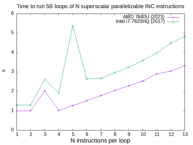
c/inc_loop_asm_n.sh results for a few CPUs
. Quite clearly:and both have low instruction count effects that destroy performance, AMD at 3 and Intel at 3 and 5. TODO it would be cool to understand those better.
- AMD 7840U can run INC on 4 functional units
- Intel i7-7820HQ can run INC on 2 functional units
Data from multiple CPUs manually collated and plotted manually with ../c/inc_loop_asm_n_manual.sh.
Announced at:
The main interface between the central processing unit and software.
List of instruction set architecture.
This ISA basically completely dominated the smartphone market of the 2010s and beyond, but it started appearing in other areas as the end of Moore's law made it more economical logical for large companies to start developing their own semiconductor, e.g. Google custom silicon, Amazon custom silicon.
It is exciting to see ARM entering the server, desktop and supercomputer market circa 2020, beyond its dominant mobile position and roots.
Ciro Santilli likes to see the underdogs rise, and bite off dominant ones.
Basically, as long as were a huge company seeking to develop a CPU and able to control your own ecosystem independently of Windows' desktop domination (held by the need for backward compatibility with a billion end user programs), ARM would be a possibility on your mind.
- in 2020, the Fugaku supercomputer, which uses an ARM-based Fujitsu designed chip, because the number 1 fastest supercomputer in TOP500: www.top500.org/lists/top500/2021/11/It was later beaten by another x86 supercomputer www.top500.org/lists/top500/2022/06/, but the message was clearly heard.
- 2012 hackaday.com/2012/07/09/pedal-powered-32-core-arm-linux-server/ pedal-powered 32-core Arm Linux server. A publicity stunt, but still, cool.
- AWS Graviton
The leading no-royalties options as of 2020.
China has been a major RISC-V potential user in the late 2010s, since the country is trying to increase its semiconductor industry independence, especially given economic sanctions imposed by the USA.
E.g. a result of this, the RISC-V Foundation moved its legal headquarters to Switzerland in 2019 to try and overcome some of the sanctions.
Leading RISC-V consultants as of 2020, they are basically trying to become the Red Hat of the semiconductor industry.
Risky name with the Si prefix, too close to SiFive. Both a reference to silicon no doubt, but still. If they stick they will one day rename.
This tutorial explains the very basics of how paging works, with focus on x86, although most high level concepts will also apply to other instruction set architectures, e.g. ARM.
The goals are to:
This tutorial was extracted and expanded from this Stack Overflow answer.
Minimal example: github.com/cirosantilli/x86-bare-metal-examples/blob/5c672f73884a487414b3e21bd9e579c67cd77621/paging.S
Like everything else in programming, the only way to really understand this is to play with minimal examples.
What makes this a "hard" subject is that the minimal example is large because you need to make your own small OS.
Although it is impossible to understand without examples in mind, try to get familiar with the manuals as soon as possible.
Intel describes paging in the Intel Manual Volume 3 System Programming Guide - 325384-056US September 2015 Chapter 4 "Paging".
Specially interesting is Figure 4-4 "Formats of CR3 and Paging-Structure Entries with 32-Bit Paging", which gives the key data structures.
Paging makes it easier to compile and run two programs or threads at the same time on a single computer.
For example, when you compile two programs, the compiler does not know if they are going to be running at the same time or not.
And thread stacks, that must be contiguous and keep growing down until they overwrite each other, are an even bigger issue!
But if two programs use the same address and run at the same time, this is obviously going to break them!
Paging solves this problem beautifully by adding one degree of indirection:
(logical) ------------> (physical)
             paging
Where:
As far as programs are concerned, they think they can use any address between 0 and 4 GiB (2^32,
FFFFFFFF) on 32-bit systems.The OS then sets up paging so that identical logical addresses will go into different physical addresses and not overwrite each other.
This makes it much simpler to compile programs and run them at the same time.
Paging achieves that goal, and in addition:
- the switch between programs is very fast, because it is implemented by hardware
- the memory of both programs can grow and shrink as needed without too much fragmentation
- one program can never access the memory of another program, even if it wanted to.This is good both for security, and to prevent bugs in one program from crashing other programs.
Or if you like non-funny jokes:

Paging is implemented by the CPU hardware itself.
Paging could be implemented in software, but that would be too slow, because every single RAM memory access uses it!
Operating systems must setup and control paging by communicating to the CPU hardware. This is done mostly via:
- the CR3 register, which tells the CPU where the page table is in RAM memory
- writing the correct paging data structures to the RAM pointed to the CR3 register.Using RAM data structures is a common technique when lots of data must be transmitted to the CPU as it would cost too much to have such a large CPU register.The format of the configuration data structures is fixed by the hardware, but it is up to the OS to set up and manage those data structures on RAM correctly, and to tell the hardware where to find them (via
cr3).Then some heavy caching is done to ensure that the RAM access will be fast, in particular using the TLB.Another notable example of RAM data structure used by the CPU is the IDT which sets up interrupt handlers. - CR3 cannot be modified in ring 3. The OS runs in ring 0. See also:
- the page table structures are made invisible to the process using paging itself!
Processes can however make requests to the OS that cause the page tables to be modified, notably:
- stack size changes
brkandmmapcalls, see also: stackoverflow.com/questions/6988487/what-does-brk-system-call-do/31082353#31082353
The kernel then decides if the request will be granted or not in a controlled manner.
In x86 systems, there may actually be 2 address translation steps:like this:
- first segmentation
- then paging
(logical) ------------------> (linear) ------------> (physical)
             segmentation                 paging
The major difference between paging and segmentation is that:
- paging splits RAM into equal sized chunks called pages
- segmentation splits memory into chunks of arbitrary sizes
This is the main advantage of paging, since equal sized chunks make things more manageable by reducing memory fragmentation problems. See also:
Paging came after segmentation historically, and largely replaced it for the implementation of virtual memory in modern OSs.
Paging has become so much more popular that support for segmentation was dropped in x86-64 in 64-bit mode, the main mode of operation for new software, where it only exists in compatibility mode, which emulates IA-32.
This is an example of how paging operates on a simplified version of a x86 architecture to implement a virtual memory space with a
20 | 12 address split (4 KiB page size).This is how the memory could look like in a single level paging scheme:
Links   Data                    Physical address

      +-----------------------+ 2^32 - 1
      |                       |
      .                       .
      |                       |
      +-----------------------+ page0 + 4k
      | data of page 0        |
+---->+-----------------------+ page0
|     |                       |
|     .                       .
|     |                       |
|     +-----------------------+ pageN + 4k
|     | data of page N        |
|  +->+-----------------------+ pageN
|  |  |                       |
|  |  .                       .
|  |  |                       |
|  |  +-----------------------+ CR3 + 2^20 * 4
|  +--| entry[2^20-1] = pageN |
|     +-----------------------+ CR3 + 2^20 - 1 * 4
|     |                       |
|     .    many entires       .
|     |                       |
|     +-----------------------+ CR3 + 2 * 4
|  +--| entry[1] = page1      |
|  |  +-----------------------+ CR3 + 1 * 4
+-----| entry[0] = page0      |
   |  +-----------------------+ <--- CR3
   |  |                       |
   |  .                       .
   |  |                       |
   |  +-----------------------+ page1 + 4k
   |  | data of page 1        |
   +->+-----------------------+ page1
      |                       |
      .                       .
      |                       |
      +-----------------------+  0
Notice that:
- the CR3 register points to the first entry of the page table
- the page table is just a large array with 2^20 page table entries
- each entry is 4 bytes big, so the array takes up 4 MiB
- each page table contains the physical address a page
- each page is a 4 KiB aligned 4 KiB chunk of memory that user processes may use
- we have 2^20 table entries. Since each page is 4 KiB == 2^12, this covers the whole 4 GiB (2^32) of 32-bit memory
Suppose that the OS has setup the following page tables for process 1:and for process 2:
entry index   entry address       page address   present
-----------   ------------------  ------------   -------
0             CR3_1 + 0      * 4  0x00001        1
1             CR3_1 + 1      * 4  0x00000        1
2             CR3_1 + 2      * 4  0x00003        1
3             CR3_1 + 3      * 4                 0
...
2^20-1 CR3_1 + 2^20-1 * 4 0x00005 1entry index entry address page address present
----------- ----------------- ------------ -------
0 CR3_2 + 0 * 4 0x0000A 1
1 CR3_2 + 1 * 4 0x12345 1
2 CR3_2 + 2 * 4 0
3 CR3_2 + 3 * 4 0x00003 1
...
2^20-1 CR3_2 + 2^20-1 * 4 0xFFFFF 1When process 1 tries to access a linear address, this is the physical addresses that will be actually accessed:
linear     physical
---------  ---------
00000 001  00001 001
00000 002  00001 002
00000 003  00001 003
00000 FFF  00001 FFF
00001 000  00000 000
00001 001  00000 001
00001 FFF  00000 FFF
00002 000  00003 000
FFFFF 000  00005 000
To switch to process 2, the OS simply sets
cr3 to CR3_2, and now the following translations would happen:linear physical
--------- ---------
00000 002 0000A 002
00000 003 0000A 003
00000 FFF 0000A FFF
00001 000 12345 000
00001 001 12345 001
00001 FFF 12345 FFF
00004 000 00003 000
FFFFF 000 FFFFF 000Step-by-step translation for process 1 of logical address
0x00000001 to physical address 0x00001001:- split the linear address into two parts:
| page (20 bits) | offset (12 bits) | - look into Page table 1 because
cr3points to it. - The hardware knows that this entry is located at RAM address
CR3 + 0x00000 * 4 = CR3:
*0x00000because the page part of the logical address is0x00000
*4because that is the fixed size in bytes of every page table entry - since it is present, the access is valid
- by the page table, the location of page number
0x00000is at0x00001 * 4K = 0x00001000. - to find the final physical address we just need to add the offset:
00001 000 + 00000 001 --------- 00001 001because00001is the physical address of the page looked up on the table and001is the offset.The offset is always simply added the physical address of the page. - the hardware then gets the memory at that physical location and puts it in a register.
Another example: for logical address
0x00001001:- the page part is
00001, and the offset part is001 - the hardware knows that its page table entry is located at RAM address:
CR3 + 1 * 4(1because of the page part), and that is where it will look for it - it finds the page address
0x00000there - so the final address is
0x00000 * 4k + 0x001 = 0x00000001
The same linear address can translate to different physical addresses for different processes, depending only on the value inside
cr3.Both linear addresses
00002 000 from process 1 and 00004 000 from process 2 point to the same physical address 00003 000. This is completely allowed by the hardware, and it is up to the operating system to handle such cases.This often in normal operation because of Copy-on-write (COW), which be explained elsewhere.
Such mappings are sometime called "aliases".
Articles were limited to the first 100 out of 416 total. Click here to view all children of Computer hardware.
Articles by others on the same topic
There are currently no matching articles.