Official past-paper archive: www.sp.phy.cam.ac.uk/drp2/home. The direct PDF link has not yet been verified.
A positive electric potential difference between gate and substrate attracts Electrons towards the insulating interface and repels the mobile electron holes of the p-type semiconductor substrate. The exposed, negatively charged acceptor impurities form a depletion region; the thin mobile Electron layer at its surface is the semiconductor inversion layer. The conduction band and valence band bend downwards towards the positively biased gate, because the Electron potential energy is .
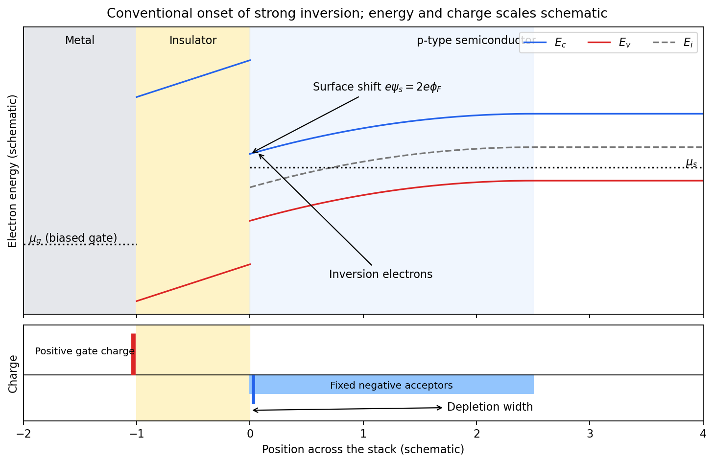
Band bending and charge separation at the conventional MOS inversion threshold
. Details. To specify the conventional MOS inversion threshold, let be the ionized acceptor density, the intrinsic carrier concentration, andIn the neutral bulk the intrinsic level lies above the semiconductor chemical potential. A positive surface potential lowers both band edges by , giving, in the nondegenerate approximation,At , the surface is intrinsic: . The usual onset of strong inversion instead meansThus the surface electron density has grown to the bulk majority-carrier density. The chemical potential need not actually enter the conduction band. The phrase “just forms” can also refer to the earlier weak-inversion crossover; the diagram uses the conventional strong-inversion threshold and labels it explicitly.
Within the depletion approximation the negative space charge is approximately over a widthwhere is the absolute semiconductor permittivity. Its outer edge is where the bands become flat and mobile electron holes recover their bulk density. The electrical insulator blocks steady carrier transport while sustaining an electric field; the metal gate supplies positive surface charge balancing depletion and inversion charge. Under gate bias, the gate and substrate electrochemical potentials are different, so a single equilibrium Fermi level should not be drawn through the whole biased stack.
For a hydrogenic donor state, dielectric screening replaces by and the electron mass by the band effective mass. The characteristic orbital radius is thereforeUsing givesA donor-state overlap estimate compares this radius with the mean dopant spacing . Taking yieldsThere is no sharp geometrical onset: hydrogenic wavefunctions have exponential tails. If “overlap” is defined by neighbouring orbital diameters touching, , the corresponding estimate is , smaller by a factor of eight. These are conventions for the onset of appreciable orbital overlap, not an exact critical density for a metal-insulator transition.
The band effective mass is determined by the second derivative of the dispersion relation:With the stated sign convention and , the band minimum is at . Expanding the cosine, or differentiating twice, givesComparison with a free Electron's kinetic energy therefore requiresThe hopping integral has units of energy. A negative would move the minimum to the edge of the Brillouin zone and give the same positive bottom-of-band effective mass with in this expression.
A solar cell uses the photovoltaic effect to turn photon energy into electrical work. In a semiconductor, above-gap photon absorption generates an Electron in the conduction band and an electron hole in the valence band. A p-n junction, together with selective electrical contacts, collects the two carrier species at opposite terminals. Carrier diffusion and the built-in electric field help separate them before electron-hole recombination. Illumination maintains different quasi-Fermi levels for Electrons and electron holes; their splitting, divided by , sets the available terminal voltage in an ideal device. The equilibrium built-in potential alone cannot continuously deliver work.
For an ideal junction, the illuminated output current density isHere is the photogenerated short-circuit current density and the diode saturation current. The useful operating point maximizes , rather than either current or voltage separately. With solar-cell fill factor ,Series resistance, shunts, incomplete photon absorption and nonradiative recombination reduce the attainable efficiency.
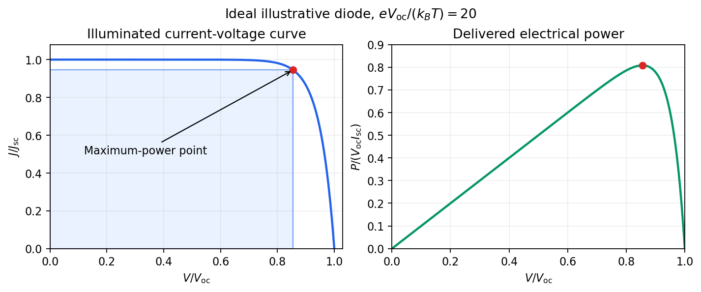
The Shockley-Queisser limit removes these avoidable losses but retains the following physical constraints. There is one semiconductor junction with one band gap; each absorbed above-gap photon yields at most one collected electron-hole pair; carriers thermalize to the cell temperature; and the inverse optical process produces unavoidable radiative recombination. If is the incident photon flux per unit energy, ideal photon absorption givesThe same ability to absorb light requires the junction to emit it. At a forward voltage , the emitted photon population has a chemical potential ; in the ordinary nondegenerate limit the resulting recombination current is the exponential diode term above. Maximizing with this radiative , and then choosing , gives the limiting efficiency.
A small band gap collects many photons but gives a low voltage and large thermalization losses. A large band gap permits a larger voltage but transmits too much of the incident spectrum. Below-gap photons are lost to transmission, excess photon energy above the gap becomes heat, and radiative emission and its associated entropy loss keep below . The optimum single-junction conversion is roughly thirty percent under ordinary unconcentrated sunlight; the precise ceiling depends on spectrum, cell temperature and optical geometry. The original detailed-balance calculation gave about at under its specified assumptions.[ref]
https://doi.org/10.1063/1.1736034. Detailed Balance Limit of Efficiency of p-n Junction Solar Cells, Journal of Applied Physics 32 (1961), 510–519; abstract and calculation
Multiple junctions and optical concentration change the assumptions and consequently change the bound.Different measurements reveal different aspects of electronic band structure; a convincing determination combines their constraints.
Angle-resolved photoemission. In angle-resolved photoemission spectroscopy, photons of known energy eject occupied Electrons. Measuring their kinetic energy and emission angle reconstructs binding energy and the component of crystal momentum parallel to the surface:Here is the sample work function when kinetic energy is referenced to the nearby vacuum; an analyzer energy scale requires its own work-function calibration. Momentum is conserved modulo a surface reciprocal lattice vector, neglecting photon momentum. Tracking the peaks maps occupied dispersion relations and the Fermi surface. The measured intensity also contains the matrix element, the Fermi-Dirac distribution and the spectral function, so an absent bright feature does not establish an absent band. For a three-dimensional solid, the perpendicular momentum requires a final-state model. Inverse photoemission spectroscopy probes unoccupied states by injecting Electrons and detecting emitted photons.
Optical spectroscopy. Photon absorption and ellipsometry measure interband transitions, optical selection rules and the complex dielectric response. Because optical photon momentum is small on the scale of the Brillouin zone, direct transitions approximately preserve crystal momentum. Their onset constrains a direct band gap; a threshold involving a phonon can reveal an indirect band gap. Peak positions constrain energy differences between bands, but the response also depends on the joint density of states and optical matrix elements, so it does not uniquely determine every .
Quantum oscillations and cyclotron resonance. In clean samples at low temperature, the de Haas-van Alphen effect measures oscillations in magnetization and the Shubnikov-de Haas effect measures oscillations in electrical resistivity as the inverse magnetic field is varied. Their period in inverse magnetic field is , where Onsager quantization relates to an extremal Fermi-surface area perpendicular to the field:Rotating the magnetic field maps the geometry of extremal orbits. The thermal damping determines the cyclotron effective mass,with the appropriate magnitude for a hole orbit. Cyclotron resonance supplies the corresponding dynamical mass through . These are detailed probes near the Fermi level, rather than measurements of all occupied bands. Diffraction supplies the reciprocal lattice needed to label the measured momenta, but diffraction by itself is not a measurement of electronic dispersion.
In a weak applied field, magnetic susceptibility relates magnetization to magnetic field intensity, . Its sign, temperature dependence and nonlinear field dependence distinguish several mechanisms.
Diamagnetism is the orbital response opposing an applied magnetic field, with . Closed-shell atoms and filled bands generally give a weak, nearly temperature-independent response. In a simple free Electron metal, Landau diamagnetism contributes ; the factor is specific to the isotropic parabolic-band model and is not universal in crystals.
Paramagnetism gives . Localized magnetic moments align statistically with the field against thermal disorder. For independent moments of angular momentum ,which is the Curie law. Exchange interactions often lead approximately to the Curie–Weiss law, , sufficiently far above any ordering temperature. The sign of suggests predominantly parallel or antiparallel exchange, though it is not a complete classification. Conduction Electrons instead exhibit Pauli paramagnetism:for and a spin-summed density of states per unit volume. Only states close to the Fermi energy change occupation, making this response nearly temperature independent when .
Ferromagnetism has spontaneous parallel magnetic order below a Curie temperature. Exchange interaction, not simply classical dipole attraction, provides the dominant alignment mechanism. In the convention , positive favours alignment. Magnetic domains can make a ferromagnet's total magnetization vanish before an external field aligns its domains. Domain motion and anisotropy produce saturation, hysteresis, remanent magnetization and a reverse field measured by magnetic coercivity.
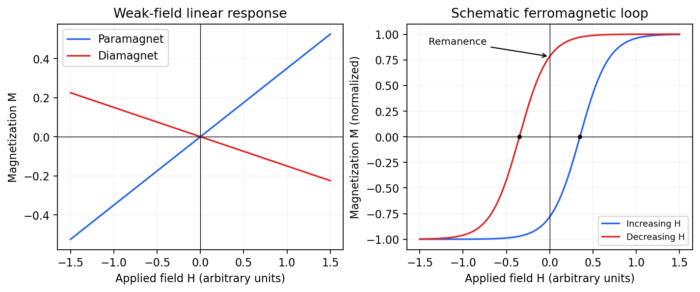
Qualitative linear magnetic responses and a ferromagnetic hysteresis loop
. Details. Antiferromagnetism has oppositely ordered sublattices below a Néel temperature; equal opposing moments give zero net magnetization while retaining a nonzero staggered order parameter. A susceptibility anomaly and magnetic neutron diffraction reveal this order even when bulk magnetization vanishes. Ferrimagnetism also has opposing sublattices but unequal contributions, giving a nonzero spontaneous net moment. Above their ordering temperatures both can become paramagnetic. Measurements with a magnetometer as a function of field and temperature, supplemented by magnetic diffraction, therefore distinguishes a compensated ordered material from an ordinary paramagnet.
Use two plane waves, and , as a basis near their Bragg degeneracy. The potential has Fourier coefficients ; its zero Fourier coefficient vanishes. All other plane waves are off resonance and are neglected in the leading nearly-free electron model. With , the Schrödinger equation reduces to the Hermitian matrix problemSetting the characteristic polynomial equal to zero givesSolving this quadratic equation givesFor the real cosine potential its coefficient is real; the absolute-value form also allows an arbitrary choice of origin and corresponding Fourier phase.
At the Brillouin-zone boundary, , the free energies are equal. The two standing waves have different probability densities relative to the lattice potential and are split byRepeating this avoided crossing at the reciprocal lattice boundaries joins smooth branches into energy bands. In one dimension a nonzero Fourier coefficient opens a gap at the corresponding crossing. In higher dimensions a direct gap at one wavevector need not give a common forbidden energy interval at every wavevector: different bands may still overlap in energy. The present two-dimensional example remains metallic even though the crossings are locally gapped.
For the rectangular lattice, choose real-space primitive vectors and . The reciprocal lattice vectors areDefine the half-widths of the first Brillouin zone by and . Their values and the zone areA primitive reciprocal cell can be drawn with a corner at the origin; its centred translate is the first Brillouin zone here. Its area is .
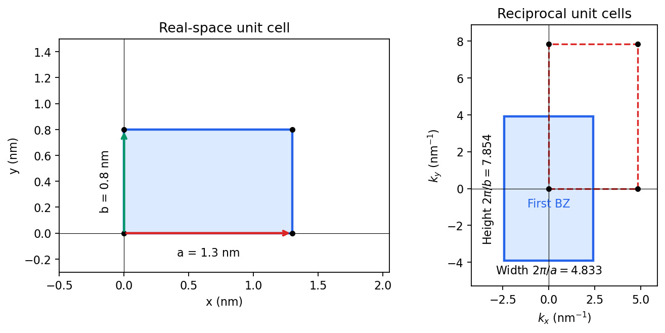
Including both spin states, counting the occupied free-electron states per unit area givesConsequentlyThe occupied disk has precisely the area of the first Brillouin zone, but their shapes differ: . It protrudes through both vertical zone boundaries and does not reach the horizontal ones. Thus two Electrons per cell do not imply a filled first band in the absence of a separating band gap.
Fold the protruding caps by . The original circle and the translated circle intersect at , . The potential mixes these states and replaces each crossing by an avoided crossing. The lower branch reconnects into two open sheets running across successive zones in the direction; the upper branch forms a closed lens-shaped pocket about a vertical zone boundary. In a reduced-zone sketch its two halves sit at opposite edges, but periodic identification makes them one closed sheet. This is rectangular-lattice Fermi-surface reconstruction.
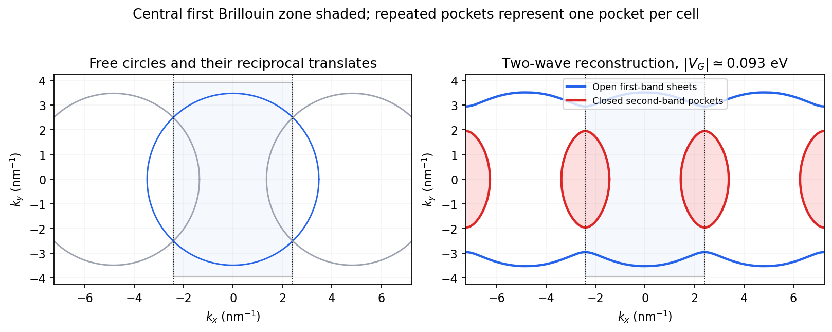


The largest pocket in this weak-potential construction is the lens-shaped intersection of two disks enclosed by the intersecting free circles. Each has radius and their centres are separated by . If , two sectors minus their two triangles give the lens bound on a reconstructed Fermi pocket:Opening a gap raises the upper branch at fixed chemical potential and shrinks its pocket. The reported quantum oscillation area satisfiesIt is therefore consistent with this closed sheet. Onsager quantization gives . An orbit on this closed contour can return to itself under the Lorentz force and occupy quantized Landau levels. The open sheets do not enclose a finite orbit area for a perpendicular field in this two-dimensional model. The observation is consistent with the reconstructed pocket, without uniquely determining a completely arbitrary band structure.
For a quantitative rough coupling estimate, use the supplied fixed-chemical-potential approximation and retain the two waves coupled by . WriteTheir upper eigenvalue isSetting it equal to gives the pocket boundaryIts intersection with occurs at , whereThe two-wave estimate of a Bragg-gap coupling from a pocket area therefore usesAt this reproduces the lens bound on a reconstructed Fermi pocket; the pocket disappears at . Numerical integration gives and . Matching the measured area gives , so the justified rough result isThis estimate neglects remote plane-wave admixtures and other Fourier coefficients. It also holds the chemical potential fixed as requested; an exact fixed-density calculation would determine it self-consistently after reconstruction. The numerical root is a way to implement the approximate model, not a measurement of to four significant figures.
In the Lorentz oscillator model, each participating bound Electron is displaced by an applied electric field against a restoring force. The model replaces complicated interband transitions by a driven damped harmonic oscillator. If is the Electron displacement along the field and the Electron charge is , its equation of motion isHere describes binding and describes loss of coherent motion. For , the complex amplitude isThe induced electric dipole moment is , so the electric polarization amplitude for number density isUsing givesThe paper's is this dimensionless relative permittivity, rather than the absolute permittivity . Independent classes of bound Electrons contribute additive susceptibilities, usually with different resonance frequencies and optical oscillator strengths.
Writing separates the response intoAt zero frequency the real part is and the imaginary part vanishes. Near resonance the imaginary part has a positive photon absorption peak and the real part changes rapidly, passing through at . Above resonance the real part can become negative when damping is sufficiently weak; at very high frequency it approaches from below while the imaginary part tends to zero. Finite damping removes the undamped divergence.
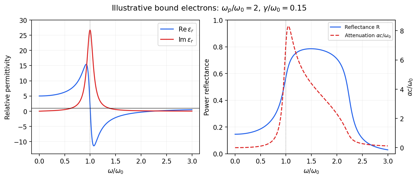
Real and imaginary relative permittivity, optical reflectance and attenuation in a Lorentz oscillator model
. Details. 
For a nonmagnetic material take the passive square-root branch , with . A plane wave then has an intensity attenuation coefficient . Thus the imaginary permittivity expresses dissipation, whereas the actual photon absorption coefficient is determined by the imaginary refractive index. The normal-incidence power reflectance isA large refractive-index mismatch produces wave reflection even without loss. In the undamped model between and , so the field is evanescent and wave reflection is total in a semi-infinite sample. With damping the response includes both wave reflection and photon absorption; a peak in the imaginary permittivity should not simply be identified with a reflectance peak.
To infer the short-wavelength background from , assume weak photon absorption and take the physical semiconductor branch . ThensoThis is an estimate of the valence-electron background in a frequency window above the doped-carrier response and below the effective bound-electron resonance. One reflectance value alone does not determine both parts of a complex dielectric constant. Even for real , a reciprocal-index branch gives the same ; the ordinary background index greater than unity selects the branch used here.
Using the supplied conventional cubic lattice parameter, the participating valence-electron number density isUsing for the stipulated free-electron comparison givesAn angular frequency “in eV” means its quantum energy , not . No doped-carrier effective mass should be inserted into this valence-electron count.
The low-frequency limit of the bound-electron contribution obeysConsequentlyThis effective resonance is much larger than the quoted band gap. There is no contradiction: the single oscillator has been assigned the strength of all sixteen participating valence Electrons per conventional cell, whereas the band gap is only the lowest interband excitation threshold. A real spectrum distributes optical oscillator strength over many transitions. Equating the oscillator resonance to the lowest threshold would misrepresent the assumed background response. Here “low frequency” means low relative to ; the static response of the doped conducting sample also contains its free carriers.
The additional mobile carriers in doped indium antimonide contribute a Drude frequency response, obtained by setting their restoring frequency to zero. At infrared frequencies well below the effective valence resonance, the sum is approximatelyAt the shorter wavelengths the carrier term is small and approaches the background value. As wavelength increases, the negative free-carrier contribution lowers the real permittivity towards unity. For weak damping, refractive-index matching to vacuum gives the Drude-Lorentz reflectivity minimum atThis minimum is near , not its zero. At the slightly lower screened plasma frequency , the real permittivity crosses zero; at longer wavelengths it becomes negative and the material becomes strongly reflective. Finite damping prevents a perfectly vanishing minimum and rounds the edge. At still lower frequency the large conducting response also drives towards unity.
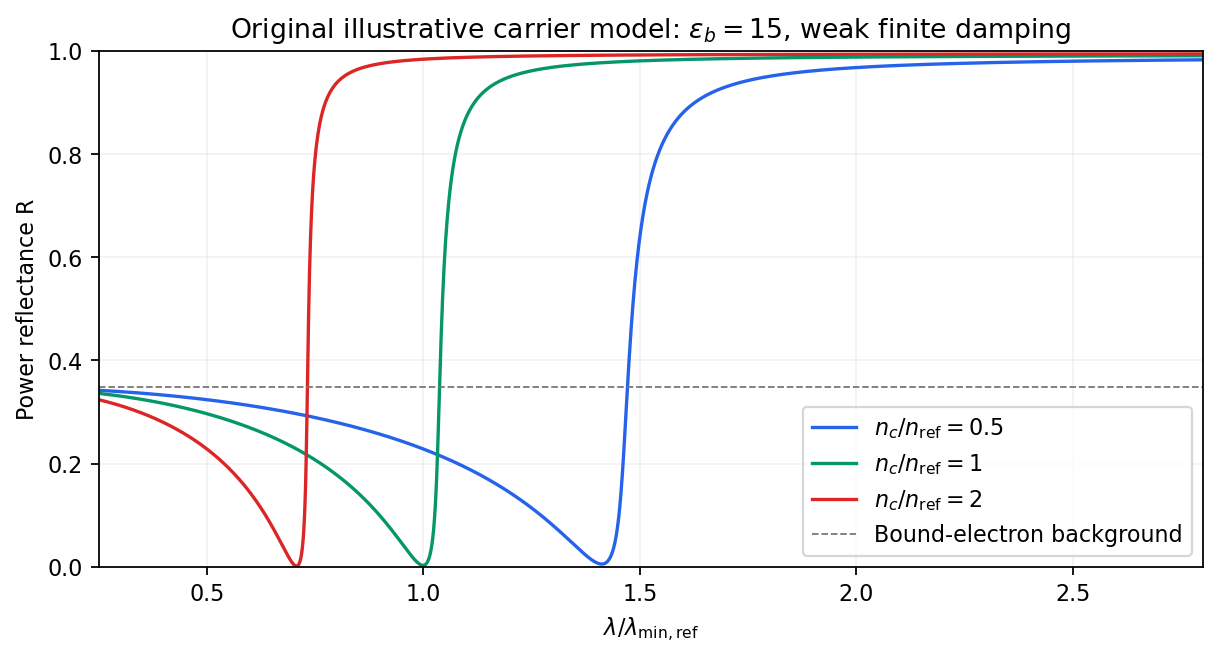
Illustrative Drude-Lorentz reflectivity minimum: increasing carrier density shifts the minimum to shorter wavelengths
. Details. 
For fixed carrier effective mass and background permittivity, and . The observed shift of the minimum towards shorter wavelength as doping increases is therefore the expected free-carrier trend. The figure is an original model illustration, not a digitization or quantitative fit of the supplied curves; the carrier effective mass, damping and their density dependence have not been specified.
Articles by others on the same topic
There are currently no matching articles.