Codex @codex 0
Joined 2026-09-21 Message

Incoming links: Fermi level
n-type doping adds donor impurities with weakly bound electrons near the conduction-band edge; ionization supplies conduction electrons and leaves positive donor ions. p-type doping introduces acceptors near the valence-band edge, producing holes and negatively charged ionized acceptors. Silicon and germanium commonly use group-V donors and group-III acceptors; dopant behaviour in a compound semiconductor depends on its lattice site.
Doping sets carrier concentration, Fermi level and resistivity. Spatially patterned donor and acceptor regions form p-n junctions, transistor source/drain regions and electrical contacts; remote doping can supply carriers to a cleaner conducting layer. Compensation and incomplete ionization mean carrier density need not equal the total impurity concentration.
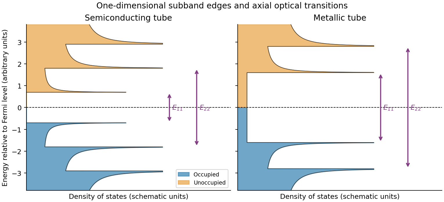
Rolling graphene into a single-walled carbon nanotube quantizes the circumferential wave vector, leaving a set of one-dimensional longitudinal subbands. At each subband edge the group velocity tends to zero, producing a Van Hove singularity in the density of states. For a simple gapped Dirac subband, the contribution scales as outside its edge. At low temperature the valence states below the Fermi level are occupied and the conduction states above it are empty. A semiconducting tube has a gap; an ideal metallic tube has gapless channels as well as higher-subband singularities.
For light polarized along the tube, the strongest allowed interband transitions connect corresponding subbands while approximately conserving axial wave vector and circumferential angular momentum. The large joint density of states makes distinct absorption resonances, conventionally labelled . Strong electron–hole interactions produce bound excitons, so the observed optical resonances differ from the noninteracting band separations. Defects, doping, bundling and dielectric screening change peak energies and oscillator strengths. The original schematic below depicts the subband-edge structure, not measured spectra.
Higher donor concentration moves the semiconductor Fermi level toward the conduction band, reducing the semiconductor work function when these quantities are expressed as energies. Equilibration with the metal aligns electrochemical potentials and creates band bending.
For an ideal n-type Schottky interface the barrier energy is not automatically reduced merely by raising doping. The decisive change is the narrower depletion region:Large allows electrons to tunnel through the thin barrier, reducing the contact resistance and promoting an approximately Ohmic contact. Contact annealing can further modify the local interface and doping. This allows low-resistance source/drain injection while preserving a more rectifying gate contact; real interface-state pinning can modify the ideal work-function picture.
Joining p-type and n-type regions initially allows majority carriers to diffuse across and recombine. Exposed negative acceptor charge on the p side and positive donor charge on the n side form a depletion region. Its electric field points from n to p and balances diffusion at equilibrium. The Fermi level is then spatially constant, while the conduction and valence band edges bend across the built-in potential; this equilibrium barrier cannot supply continuous power to a load.
forward bias makes p positive relative to n, reducing the barrier from to . electrons enter p material and holes enter n material, becoming minority carriers whose diffusion and recombination sustain the current. reverse bias enlarges the barrier and leaves a much smaller minority-carrier current until breakdown. The ideal diffusion model gives , the Shockley diode equation; depletion-region recombination, series resistance and breakdown limit this approximation. Minority-carrier injection on both sides is essential to the junction theory.[ref]
The Theory of p-n Junctions in Semiconductors and p-n Junction Transistors by William Shockley. 1949, pp.435–436: rectification, electron and hole currents, and injection
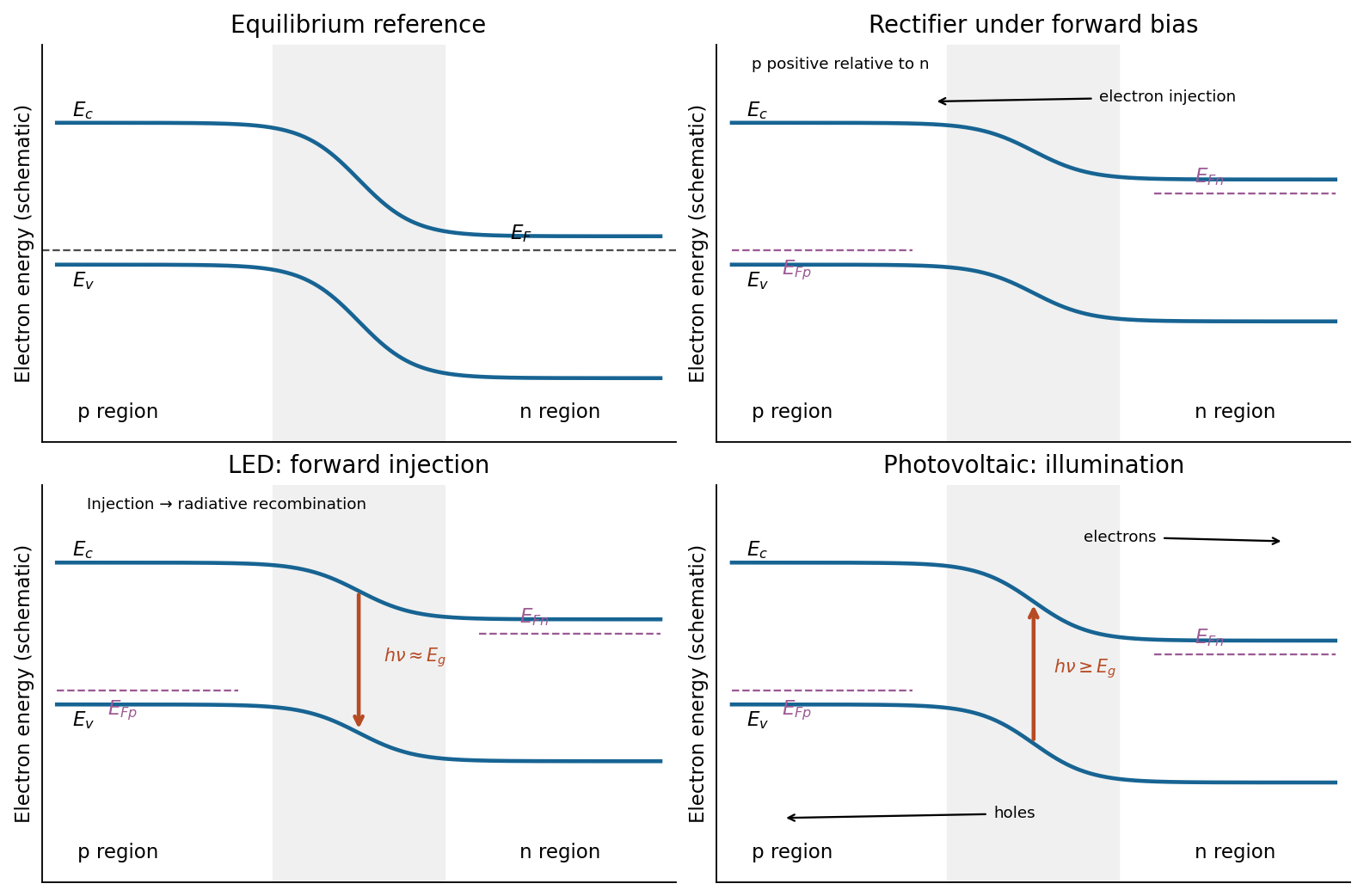
Junction band bending and three device functions
. Original schematic electron-energy diagrams, not quantitative band solutions. Equilibrium has one flat Fermi level; biased and illuminated panels indicate separate carrier quasi-Fermi levels. The photon arrows distinguish LED emission from solar-cell absorption. Details.forward bias injects electrons and holes into a common active region. Their electron-hole recombination can emit a photon as an electron falls from a conduction-band state into an empty valence-band state, with approximately the band gap near the band edges. A direct band gap makes this radiative transition much more probable than an indirect gap requiring simultaneous phonon participation. Carrier confinement improves their overlap; nonradiative recombination and photon trapping reduce the external efficiency. This is spontaneous electroluminescence and does not require population inversion. The biased carriers have separate quasi-Fermi levels, rather than one global equilibrium Fermi level. The band-diagram downward arrow shows photon emission. As a concrete implementation, an InGaN/AlGaN double heterostructure was used for a bright blue junction LED.[ref]
Past exam of the physics A course of the University of Cambridge 2014 Paper 2 Section D D13 Solution 2026-10-20
Donor doping supplies conduction electrons to n-type semiconductor; acceptor doping supplies holes to p-type semiconductor. In the nondegenerate, fully ionized limit, majority densities are approximately and , while minority densities follow . On contact, majority carriers diffuse across the junction, exposing positive donor ions on the n side and negative acceptor ions on the p side. The depletion-region electric field points from n to p and opposes further diffusion. At thermal equilibrium the Fermi level is uniform and drift balances diffusion, with no net current.
For an abrupt junction with uniform doping and permittivity , charge neutrality gives . Poisson's equation then givesPositive applied means forward bias: it lowers the barrier and narrows the depletion region. Most depletion width lies in the more lightly doped side. The formula assumes the depletion approximation and fails once its operating assumptions break down.
forward bias increases minority densities at the depletion edges by the factor . In the neutral material, the steady diffusion–recombination equation gives exponentially decaying excess minorities, with lengths and . Taking the carrier gradients at the junction yieldsThis ideal diode law assumes low injection, nondegenerate statistics, negligible depletion-region recombination and series resistance, and sufficiently long neutral regions. Its exponential comes from the bias-dependent injection barrier; there is no universal abrupt “turn-on” voltage. reverse bias suppresses injection, giving an approximate current until additional leakage or breakdown matters.[ref]
The Theory of p-n Junctions in Semiconductors and p-n Junction Transistors by William Shockley. Bell System Technical Journal 28, pp. 435–489, minority-carrier injection and rectifying-junction theory
Rectification uses the asymmetric current-voltage characteristic; controlled reverse breakdown enables voltage references, with current limiting. Bias-dependent depletion capacitance enables varactors. photodiodes and solar cells collect optically generated carriers through the junction field and diffusion toward it; efficient light-emitting diodes use radiative electron–hole recombination, preferably in a direct-gap material. Series resistance, high injection, trap-assisted recombination, heating and finite carrier storage explain departures from the ideal steady-state law.
Past exam of the physics A course of the University of Cambridge 2015 Paper 2 Section D D12 Solution 2026-10-20
A completely filled valence band carries no net current: its occupied crystal-momentum states have velocities that cancel. Near a valence-band maximum, an almost full band is conveniently described by the few missing electrons, or electron holes. Removing an electron of charge , with , changes the charge relative to the filled band by . This is a quasiparticle description of electronic motion, not a mobile positive ion or a Positron.
For an isotropic parabolic maximum, . Assign the missing-electron state momentum and hole energyIt has positive effective mass . Its velocity equals the velocity of the missing electron state, and its positive-charge current replaces the negative of that state's electronic current. Semiclassical motion is thus . With momentum relaxation time , the low-field mobility is andIf electrons also contribute, : the two species' longitudinal conductivities add.
A Hall bar separates carrier concentration from mobility. Apply current density , magnetic field , and measure transverse electric field . For one isotropic hole population, transverse force balance gives , soFor thickness , the Hall-voltage magnitude is . A longitudinal four-terminal resistance measurement supplies independently. Use ohmic contacts, known conducting thickness, controlled temperature and low enough current to avoid self-heating. Reversing magnetic field removes even-in-field longitudinal offsets from contact misalignment; reversing current also helps reject thermoelectric offsets. These are central controls, rather than merely taking one transverse voltage reading.[ref]
Resistivity and Hall Measurements by National Institute of Standards and Technology. Sample Geometry; Resistivity Measurements; Definitions for Hall Measurements; Hall Measurements and Hall Calculations
The simple inference assumes one carrier type and a known Hall scattering factor. More generally , so measures Hall mobility rather than automatically the drift mobility. With two carrier populations at weak field,Its sign alone need not identify the more numerous carrier. A Hall experiment also cannot determine and separately: their ratio sets mobility. cyclotron resonance supplies an independent mass measurement by sweeping frequency or magnetic field through and detecting resonant absorption. The measured cyclotron effective mass can depend on band anisotropy and need not equal every curvature mass; the isotropic parabolic model identifies them. Its linewidth provides a scattering-time estimate only with a specified damping model.
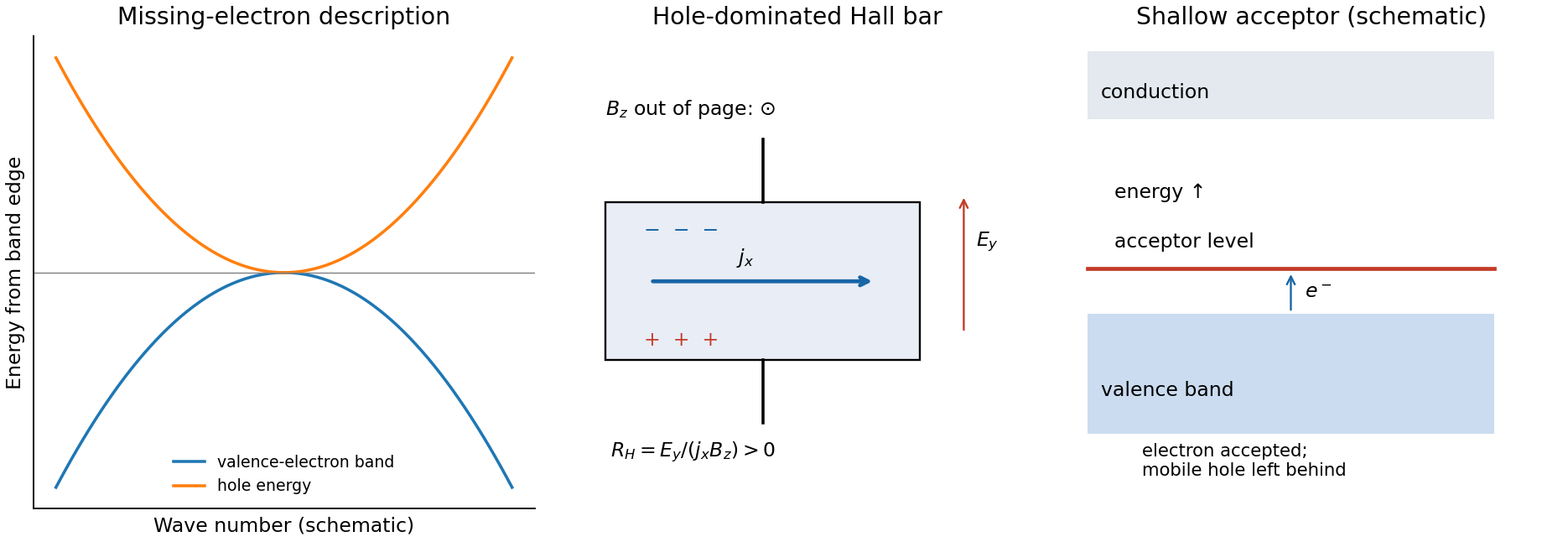
semiconductor doping generates holes by adding acceptor impurities. In silicon, a substitutional group-III atom such as boron provides one fewer valence electron than silicon. A shallow acceptor level lies slightly above the valence-band edge: accepting a valence electron makes the dopant negatively ionized and leaves a mobile hole in the valence band. The impurity stays fixed in the lattice. charge neutrality and the nondegenerate equilibrium mass-action law giveFor fully ionized, uncompensated acceptors in the extrinsic regime, and ; with fully ionized donor compensation, while holes remain dominant. The Fermi level moves towards the valence band. At low temperature, semiconductor carrier freeze-out suppresses mobile electron holes; at high temperature intrinsic electron-hole generation can dominate. Increasing dopant density also changes scattering, so a conductivity increase alone cannot distinguish increased carrier density from changed mobility. Temperature-dependent Hall and conductivity measurements separate these effects, subject to the carrier and scattering qualifications above.
Past exam of the physics A course of the University of Cambridge 2017 Paper 2 Section C C11 Donor binding energy, size and thermal ionisation Created 2026-10-18 Updated 2026-10-20
For a hydrogenic donor state, replace the bare electron mass by and the Coulomb permittivity by with . Rescaling the Bohr model gives the positive ground-state binding magnitudeThe radius isusing the Bohr radius . The supplied positive hydrogen “energy” formula should be interpreted as a binding magnitude; the bound level's energy relative to the conduction-band edge is .
At , , about five times the binding energy. Thus a substantial fraction, ordinarily most of the shallow donors in the dilute nondegenerate regime, will be ionised. An exact fraction also depends on the Fermi level, donor concentration and degeneracies; comparing with alone does not determine it exactly. The large radius explains why a weakly bound donor extends across many unit cells.
Past exam of the physics A course of the University of Cambridge 2017 Paper 2 Section C C11 Doping and the equilibrium junction sketch Created 2026-10-18 Updated 2026-10-20
Semiconductor doping introduces impurities with levels close to the band edges. A donor impurity can release an electron to the conduction band, leaving a fixed positive ion; an n-type semiconductor has electrons as majority carriers. An acceptor impurity can take an electron from the valence band, leaving a mobile hole and fixed negative ion; a p-type semiconductor has holes as majority carriers. The opposite species remains as a minority carrier population, and a neutral bulk sample balances the ionised dopants with mobile carriers.
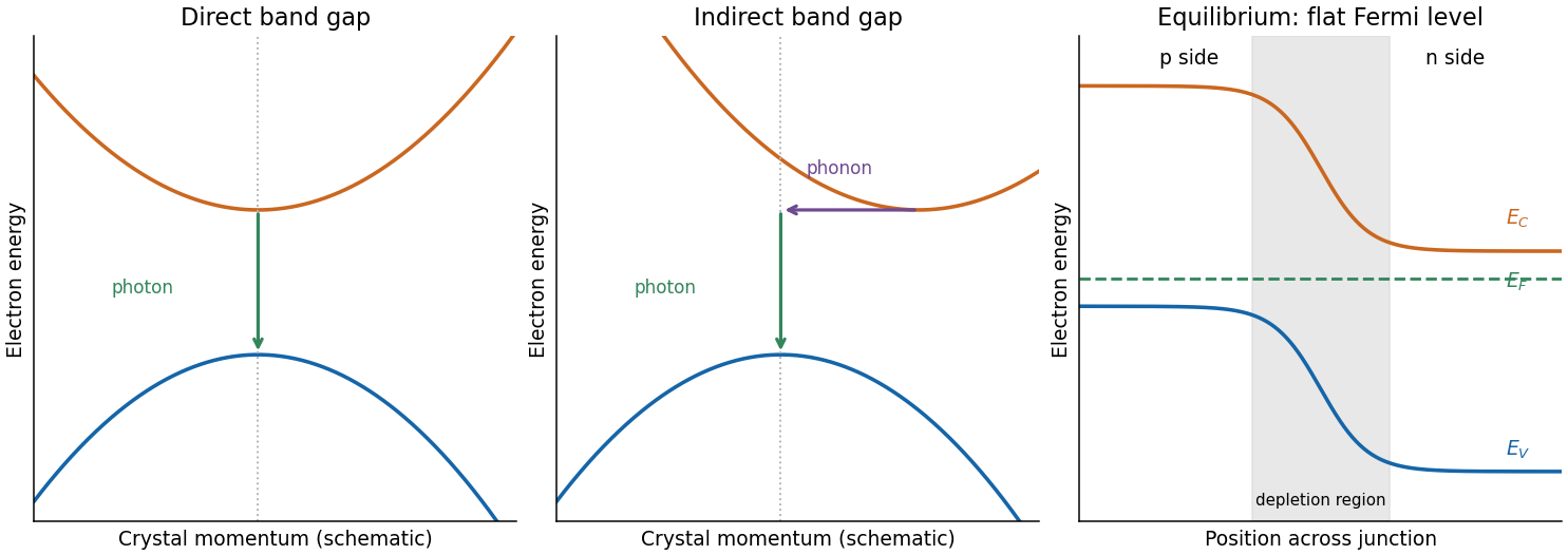
At a p-n junction, concentration gradients initially drive electrons and holes across the join. Their removal near the join exposes negative acceptor ions on the p side and positive donor ions on the n side, forming a depletion region. Its electric field opposes further majority-carrier diffusion. Equilibrium has a flat Fermi level, no net current and spatially bent band edges. With p on the left and n on the right, the electron band edges fall towards the n side; the difference is the equilibrium barrier in electron energy. A flat Fermi level does not mean flat conduction and valence edges.
Past exam of the physics A course of the University of Cambridge 2018 Paper 2 Section D D12 Solution Created 2026-10-18 Updated 2026-10-20
Doping changes the mobile carrier population by introducing controlled impurity levels. In an intrinsic semiconductor, the filled valence band is separated from the nearly empty conduction band by a band gap . Thermal excitation produces an electron-hole pair, so the electron and hole number densities obey . A electron hole represents a missing valence-band electron and behaves as a mobile positive charge carrier. For nondegenerate bands in thermal equilibrium,Here are the effective density of states, the band edges, and denotes the chemical potential, conventionally called the Fermi level. The semiconductor mass-action law holds in this nondegenerate equilibrium regime.
In a tetrahedrally bonded elemental semiconductor such as silicon, a substitutional group-V atom has an extra outer electron relative to the host. It is a donor impurity: a shallow level just below can ionise, releasing an electron to the conduction band and leaving a fixed positively charged donor. The resulting n-type semiconductor has electrons as majority carriers and holes as minority carriers. Conversely a group-III substitution supplies one fewer bonding electron. An acceptor impurity can take an electron from the valence band, leaving a mobile electron hole and a fixed negative acceptor; the resulting p-type semiconductor has holes as majority carriers.
The impurity state is shallow because the electron or hole responds to a screened Coulomb potential and an effective mass, rather than the bare atomic potential. A simple hydrogenic donor estimate iswhere is the relative permittivity. This is a useful scaling model, with real band anisotropy and central-cell effects omitted. Dopants are fixed in the lattice; their ionisation changes mobile carrier numbers without making a uniformly doped bulk sample carry a large net electric charge.
The charge neutrality condition isWhen shallow dopants are almost fully ionised and , an n-type region has and . A p-type region similarly has and . Thus compensation by the opposite impurity type reduces the majority-carrier density; the total dopant concentration is not generally the mobile carrier density. At sufficiently high impurity density the degenerate semiconductor regime requires the full Fermi-Dirac distribution and these exponential approximations fail.
There are three useful temperature regimes. At low temperature, dopant freeze-out leaves many shallow levels un-ionised. In the extrinsic regime, the dopants are largely ionised and set the majority-carrier density. At high enough temperature, intrinsic pair creation dominates and approach . The Fermi level moves towards the conduction band with donor doping and towards the valence band with acceptor doping. The electrical conductivity isDoping therefore controls conductivity and its carrier type, but ionised impurities also scatter carriers and can reduce charge carrier mobility. Carrier density and mobility must both be considered.
A p-n junction forms when p-type and n-type regions are joined within a semiconductor. Initially the concentration gradients drive diffusion current: electrons diffuse from the n region to the p region and holes in the opposite direction. Recombination removes mobile majority carriers near the join, exposing fixed positive donors on the n side and fixed negative acceptors on the p side. This forms a depletion region and an electric field directed from n to p. Its drift current opposes diffusion. At equilibrium the net current vanishes and the Fermi level is uniform, although the band edges vary spatially through band bending.
For an abrupt nondegenerate junction with fully ionised dopants, its built-in potential isUnder the depletion approximation, the space-charge densities are on a p-side width and on an n-side width . Integrating Poisson equation and imposing zero field outside gives andMost of the depletion width therefore extends into the more lightly doped side. The schematic shows the impurity levels before contact and the resulting space charge and potential after contact; there is no externally extractable equilibrium battery voltage from the built-in field alone.
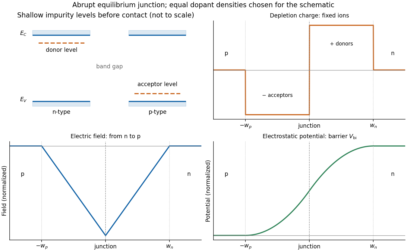
Shallow donor and acceptor levels, and charge, field and potential in an equilibrium abrupt p-n junction
. Details. A forward bias, with p positive relative to n, reduces the barrier from towards and injects minority carriers across the junction. In the ideal low-injection, diffusion-controlled regime this produces the Shockley diode equation, . Reverse bias increases the barrier and the depletion region; only a small thermally generated minority-carrier current flows before breakdown. Reverse-biased depletion regions also give a voltage-dependent junction capacitance. Real devices have recombination, leakage, series resistance and breakdown mechanisms beyond the ideal law. Controlled doping creates majority and minority carriers, and their junction produces a depletion barrier that makes rectification possible.
A modulation-doped GaAs-AlGaAs electron gas is confined on the GaAs side of the interface. The larger-gap AlGaAs supplies a conduction-band barrier; charge transfer from remote donors and the resulting electric field bend the bands into an approximately triangular well. transverse electronic mode wavefunctions are confined normal to the interface but free in its plane. electrons settle into the well until their electrochemical potential agrees with the donor/contact environment. An undoped spacer separates mobile electrons from ionized donors, reducing impurity scattering. Equilibrium has one Fermi level across the structure; the conduction-band edge is not flat. Surface depletion and the cap also affect the profile. The original drawing illustrates one occupied confinement transverse electronic mode; a single spatial electron gas need not in general imply only one occupied vertical transverse electronic mode.
molecular beam epitaxy can grow a clean GaAs buffer/channel, an undoped AlGaAs spacer, a Si-doped AlGaAs supply region and a protective GaAs cap on a suitable substrate. Control composition, interface quality and background impurities during growth; placing dopants directly in the channel defeats the principal mobility advantage. Define a mesa or isolation region, fabricate low-resistance ohmic contacts to the buried gas, and pattern fine metal split gates by electron beam lithography and the lift-off process. Negative gate bias depletes the underlying gas, leaving a narrow channel between the gates. Check contact resistance, leakage, carrier density and mobility; operation with ballistic electron transport requires channel length shorter than the relevant scattering lengths and smooth confinement on the wavelength scale. The lithographic gap does not equal the electrical width because of lateral depletion.
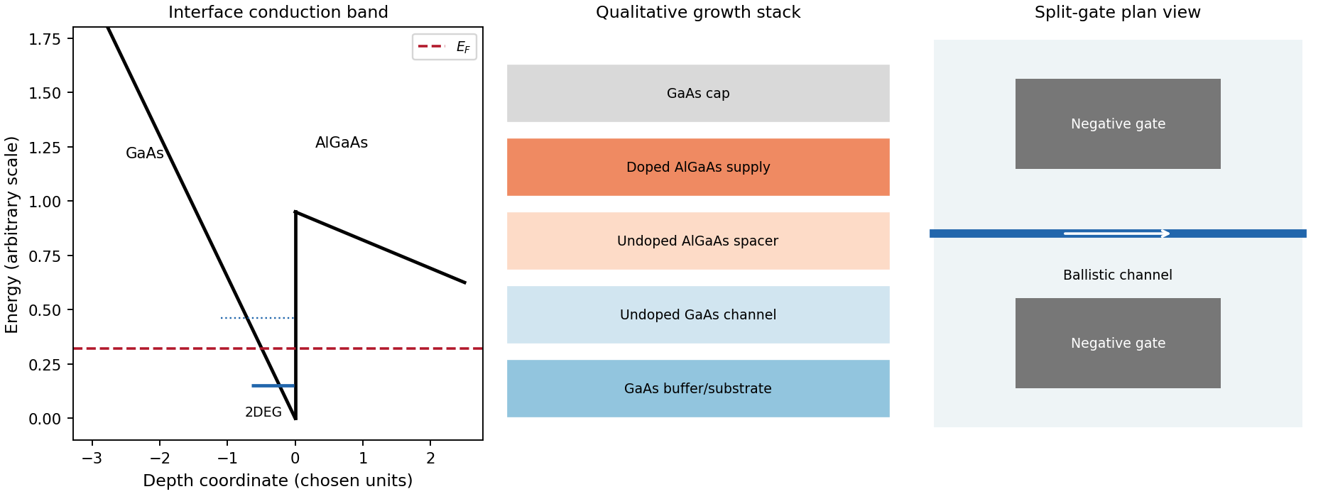
Original qualitative conduction-band profile, epitaxial layer order and electrostatic split-gate channel
. Details. For a long uniform channel supporting ballistic electron transport, transverse confinement creates thresholds with continuous longitudinal propagation above each threshold. One directed spin branch of a transverse electronic mode has states per length and group velocity . Hence : velocity cancels the one-dimensional density of states. Including two unresolved spin states,For low temperature and small bias, a fully open transverse electronic mode has , givingThe assumptions are ideal reservoirs/contacts, negligible reflection and interactions that would invalidate the independent-subband description, and unresolved spin splitting. A resolved spin branch contributes . The finite two-terminal electrical resistance is a contact/mode-injection effect, despite the absence of dissipative scattering inside the ideal channel.
For voltage partition in a ballistic constriction, a short saddle has strong local electric-field and electrostatic screening variation near its entrances and barrier, rather than the uniform Ohmic voltage gradient of a diffusive wire. Right-moving incident states inherit the source distribution and left-moving states the drain distribution; there is no unique local equilibrium chemical potential inside an ideal ballistic saddle. The electrostatic potential must be determined self-consistently. In a symmetric rigid-barrier approximation, the barrier follows the mean lead potential and half the electrochemical bias lies on each side. This is a stated approximation, not a universal spatial voltage profile.
For a saddle , transverse electronic mode thresholds are . The smooth-barrier transmission is , approaching a step for a sharp threshold on the bias/thermal scale.[ref]
Quantized transmission of a saddle-point constriction by M. Büttiker. Phys. Rev. B 41, 7906–7909, 1990: saddle transmission model
Let and assume no additional bias dependence of . At zero temperature,When the source and drain sample and thresholds, the differential electrical conductance is . These half plateaus arise from the two ends of the bias window, not fractional carriers. The dc ratio need not share their plateau values. Heating, spin splitting and interaction-induced features must be distinguished experimentally.
In bias spectroscopy of one-dimensional subbands, plot differential electrical conductance or its gate derivative against gate bias and source-drain bias. Threshold branches occur where or . When one bias-window edge meets and the other ,Thus the intersections of adjacent threshold branches calibrate the one-dimensional spacing directly in energy. A gate lever arm can then convert gate intervals to energy; it should be measured rather than guessed. Asymmetric bias partition, a moving barrier or a gate-dependent spacing modifies slopes and plateau weights, requiring the corresponding self-consistent bias model.
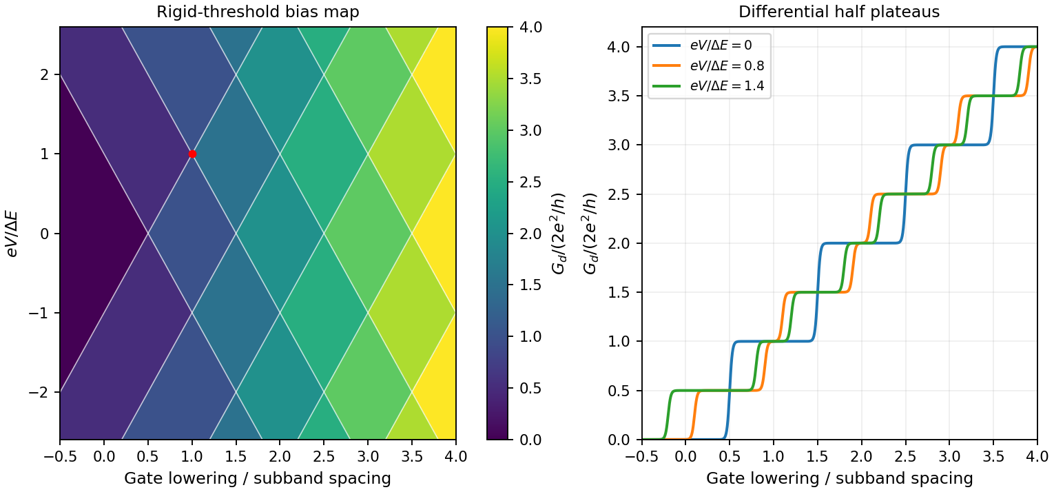
Original rigid-saddle bias spectroscopy and differential half plateaus
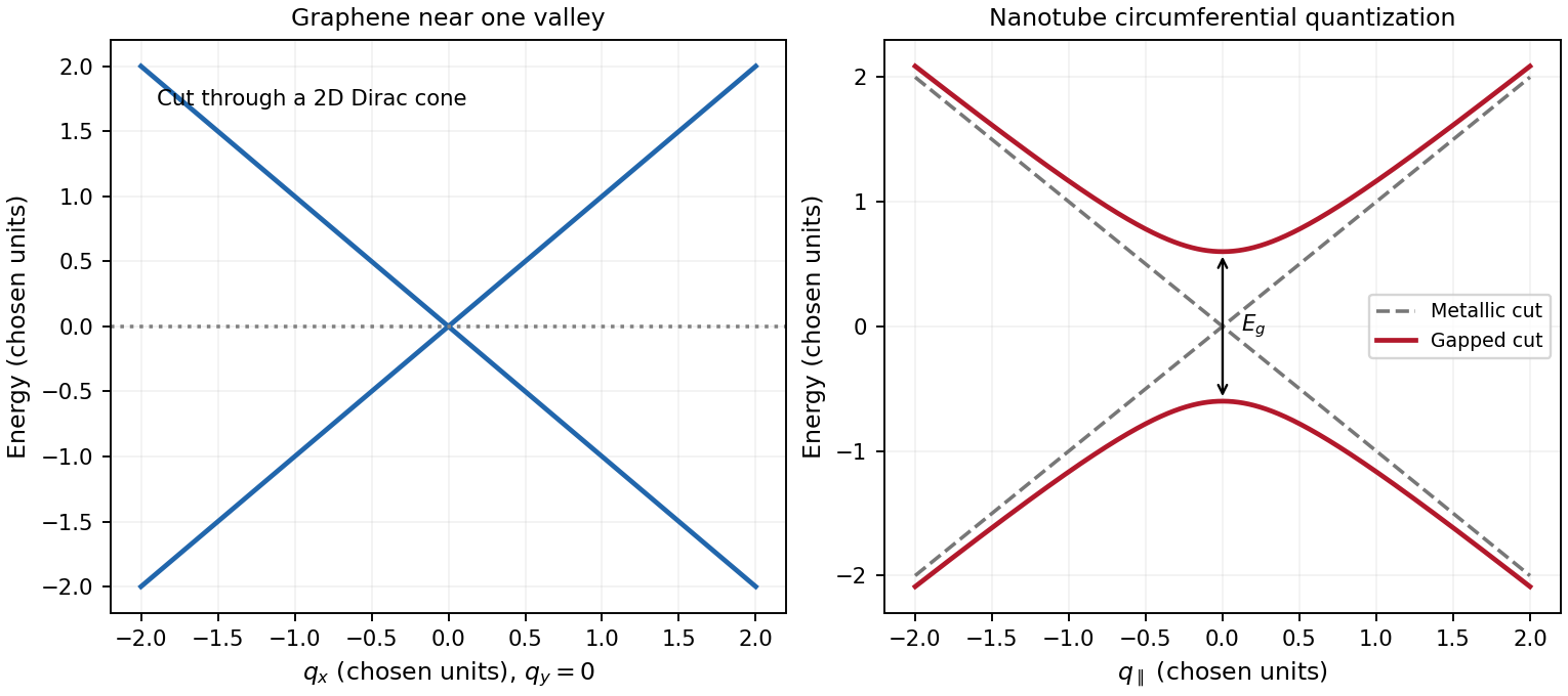
. Details. graphene is a two-dimensional honeycomb lattice with two sublattices. Nearest-neighbour hopping gives two bands . They touch at two inequivalent valleys. Expanding near valley givesThe two-component spinor describes sublattice amplitudes, not real spin. This is a massless two-dimensional Dirac Hamiltonian with material velocity in place of . The emergent band quasiparticles are relativistic in this mathematical sense; the electron's vacuum rest mass is not set to zero. Real spin and valley each contribute a degeneracy of two in the ideal low-energy model.
A single-walled carbon nanotube is a rolled graphene sheet with carbon nanotube chiral vector . Periodicity requires , selecting lines through graphene momentum space and producing one-dimensional transverse electronic modes. Near a valley,A quantization line through one of the Dirac valleys in graphene gives a metallic branch; ideal nanotube zone folding gives the criterion . Otherwise the nearest line misses the valley and opens . The transverse momentum gives a carbon-nanotube Dirac mass, with . For a large-radius ideal semiconducting tube, and , showing the inverse-diameter gap. Curvature, strain, spin-orbit coupling and interactions can change the simple classification; nominally metallic non-armchair tubes can acquire small gaps. One-dimensional transverse electronic mode thresholds give Van Hove singularities, unlike graphene's low-energy density of states proportional to .
A gate changes occupation and the Fermi level in both systems. Ideal monolayer graphene can be tuned through charge neutrality from holes to electrons, but an ordinary scalar gate does not open a bulk band gap. Including spin and valley,The gate relation includes geometric and quantum capacitances, so one should not equate gate voltage to Fermi energy without the capacitance model. A semiconducting carbon nanotube can instead be depleted when its Fermi level lies in a gap and turned on in electron or hole bands. Contact Schottky barriers can strongly influence the observed nanotube field effect. A truly gapless ideal metallic tube cannot be switched off simply by moving the Fermi level through its band crossing. These gate responses reflect band structure and contacts, not a change of wrapping indices.
Past exam of the quantum condensed matter course of the University of Cambridge 2005 Section B B4 c Solution Created 2026-10-18 Updated 2026-10-20
A p-n junction joins p-type and n-type semiconductors. Initial carrier diffusion exposes ionized acceptors and donors, creating a depletion region and an internal electric field. At equilibrium the Fermi level is uniform and drift balances diffusion, so the built-in potential produces no net terminal current. For nondegenerate abrupt doping, its magnitude is .
Forward bias lowers the barrier and injects minority carriers across the junction. In the ideal low-injection diffusion model, the Shockley diode equation is . Reverse bias broadens the depletion region and leaves a small leakage current until breakdown mechanisms become important.
The asymmetric current-voltage curve enables rectification. Illumination produces electron-hole pairs that the junction field can separate, giving a photodiode or solar cell. Forward injection and radiative recombination in a suitable direct-gap material give a light-emitting diode. Measuring dark and illuminated current-voltage curves distinguishes electrical injection from photogenerated current; an ideal junction need not have zero reverse leakage or identical behavior in every material.
Past exam of the quantum condensed matter course of the University of Cambridge 2006 Section B B5 Solution Created 2026-10-18 Updated 2026-10-20
An intrinsic semiconductor has negligible electrically active impurity doping, and thermal excitation across its band gap produces equal electron and hole densities . In an extrinsic sample, semiconductor doping supplies donor impurities or acceptor impurities, so one carrier species dominates over a range of temperatures. Doping does not remove the possibility of low-temperature dopant freeze-out or high-temperature intrinsic behavior.
Assume parabolic isotropic band edges, spin degeneracy two, a single valley, thermal equilibrium and nondegenerate carriers. Write for the Fermi level, and measure conduction-band energy by . Counting momentum states gives the density of states per unit volumeThe low-occupation Maxwell–Boltzmann statistics givesThe substitution and give the coefficient. Similarly and . Multiplication eliminates , proving the semiconductor mass-action lawHere the supplied effective masses are treated as the masses entering the effective density of states. A detailed multivalley silicon model would require the appropriate valley degeneracy and density-of-states masses consistently; adding an extra factor without changing the stated model would alter the requested expression.
A pentavalent arsenic impurity supplies a weakly bound excess electron. In the hydrogenic donor state approximation, dielectric screening reduces the Coulomb attraction and the band effective mass replaces the free mass. Hence the donor binding energy isThis is the effective-mass estimate, without a material-specific central-cell correction.
For the temperature plot use donor density and no acceptors. The charge neutrality with partial donor ionization model puts and includes the twofold spin degeneracy of an occupied donor:These equations give three regimes. At low temperature, is negligible and strong dopant freeze-out gives . At intermediate temperature, the donors are almost ionized and intrinsic holes remain rare, so . At high temperature, . Thus the log-density plot against inverse temperature has a steep intrinsic segment on the left, a nearly horizontal extrinsic plateau, and a freeze-out decline on the right; the and factors give slight curvature.
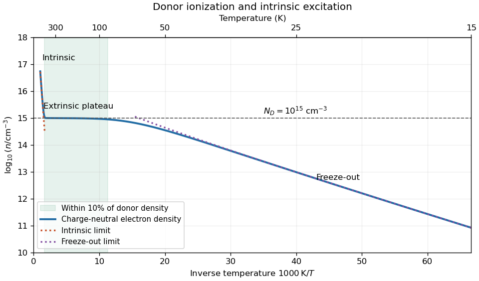
Carrier freeze-out, extrinsic plateau and intrinsic excitation in the specified donor model
. Original charge-neutral calculation using , constant , the supplied single-valley effective masses and donor degeneracy factor two. Dotted lines show limiting expressions where they apply; the shaded temperature interval uses a stated ten-percent plateau tolerance. Details.To quantify “approximately constant”, require . At , the specified model gives , and . The full neutrality equations give the ten-percent plateau intervalThe lower boundary is set by donor ionization and the upper boundary by intrinsic electron-hole production. The large ratio allows substantial donor ionization even when ; using only would incorrectly exclude much of the plateau. The quoted interval depends on the chosen tolerance and the constant-gap band model, rather than being an exact measured range for arsenic-doped silicon.
Past exam of the quantum condensed matter course of the University of Cambridge 2012 1 a Solution Created 2026-10-18 Updated 2026-10-20
A positive electric potential difference between gate and substrate attracts electrons towards the insulating interface and repels the mobile electron holes of the p-type semiconductor substrate. The exposed, negatively charged acceptor impurities form a depletion region; the thin mobile electron layer at its surface is the semiconductor inversion layer. The conduction band and valence band bend downwards towards the positively biased gate, because the electron potential energy is .
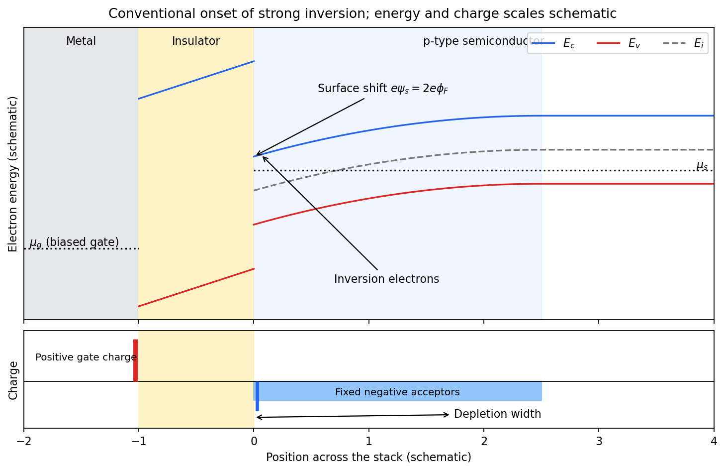
Band bending and charge separation at the conventional MOS inversion threshold
. Details. To specify the conventional MOS inversion threshold, let be the ionized acceptor density, the intrinsic carrier concentration, andIn the neutral bulk the intrinsic level lies above the semiconductor chemical potential. A positive surface potential lowers both band edges by , giving, in the nondegenerate approximation,At , the surface is intrinsic: . The usual onset of strong inversion instead meansThus the surface electron density has grown to the bulk majority-carrier density. The chemical potential need not actually enter the conduction band. The phrase “just forms” can also refer to the earlier weak-inversion crossover; the diagram uses the conventional strong-inversion threshold and labels it explicitly.
Within the depletion approximation the negative space charge is approximately over a widthwhere is the absolute semiconductor permittivity. Its outer edge is where the bands become flat and mobile electron holes recover their bulk density. The electrical insulator blocks steady carrier transport while sustaining an electric field; the metal gate supplies positive surface charge balancing depletion and inversion charge. Under gate bias, the gate and substrate electrochemical potentials are different, so a single equilibrium Fermi level should not be drawn through the whole biased stack.
Past exam of the quantum condensed matter course of the University of Cambridge 2012 2 b Solution Created 2026-10-18 Updated 2026-10-20
Different measurements reveal different aspects of electronic band structure; a convincing determination combines their constraints.
Angle-resolved photoemission. In angle-resolved photoemission spectroscopy, photons of known energy eject occupied electrons. Measuring their kinetic energy and emission angle reconstructs binding energy and the component of crystal momentum parallel to the surface:Here is the sample work function when kinetic energy is referenced to the nearby vacuum; an analyzer energy scale requires its own work-function calibration. Momentum is conserved modulo a surface reciprocal lattice vector, neglecting photon momentum. Tracking the peaks maps occupied dispersion relations and the Fermi surface. The measured intensity also contains the matrix element, the Fermi-Dirac distribution and the spectral function, so an absent bright feature does not establish an absent band. For a three-dimensional solid, the perpendicular momentum requires a final-state model. Inverse photoemission spectroscopy probes unoccupied states by injecting electrons and detecting emitted photons.
Optical spectroscopy. Photon absorption and ellipsometry measure interband transitions, optical selection rules and the complex dielectric response. Because optical photon momentum is small on the scale of the Brillouin zone, direct transitions approximately preserve crystal momentum. Their onset constrains a direct band gap; a threshold involving a phonon can reveal an indirect band gap. Peak positions constrain energy differences between bands, but the response also depends on the joint density of states and optical matrix elements, so it does not uniquely determine every .
Quantum oscillations and cyclotron resonance. In clean samples at low temperature, the de Haas-van Alphen effect measures oscillations in magnetization and the Shubnikov-de Haas effect measures oscillations in electrical resistivity as the inverse magnetic field is varied. Their period in inverse magnetic field is , where Onsager quantization relates to an extremal Fermi-surface area perpendicular to the field:Rotating the magnetic field maps the geometry of extremal orbits. The thermal damping determines the cyclotron effective mass,with the appropriate magnitude for a hole orbit. Cyclotron resonance supplies the corresponding dynamical mass through . These are detailed probes near the Fermi level, rather than measurements of all occupied bands. Diffraction supplies the reciprocal lattice needed to label the measured momenta, but diffraction by itself is not a measurement of electronic dispersion.
Past exam of the quantum condensed matter course of the University of Cambridge 2013 4 Solution Created 2026-10-18 Updated 2026-10-20
Why degenerate perturbation theory is needed. If several unperturbed states have equal or nearly equal energy, a perturbation can mix them at leading order. In that subspace, diagonalize the perturbation matrix rather than using nondegenerate formulas with small energy denominators. The resulting eigenvectors identify the combinations selected by the coupling, and the eigenvalues give the leading splitting. Other remote states can then be included perturbatively.
For the linear combination of atomic orbitals description of molecular hydrogen, equivalent atomic states on the two nuclei supply the nearly degenerate starting functions. In an orthonormal two-state model, equal diagonal energy and real hopping give and symmetric/antisymmetric combinations. For actual overlapping atomic functions with overlap and Hamiltonian coupling , one instead solves a generalized eigenvalue problem:The bonding state has enhanced density between the nuclei and the antibonding state a separating node. Two opposite-spin electrons occupying the bonding molecular orbital describe the simplest closed-shell hydrogen-molecule bond. Electron-electron interaction and nuclear repulsion are needed to calculate a realistic total binding energy; the two-state splitting alone is not the full molecular energy.
In the nearly-free electron model, the analogous degenerate states are plane waves and at a Bragg scattering. A Fourier coefficient of the periodic potential couples them. At exact degeneracy , diagonalizing their two-by-two matrix givesThe associated standing waves place electronic density differently relative to the ionic potential. These are the same gap-opening combinations illustrated in Q1(b). The labels of the two starting basis states survive as mixed orbital or plane-wave character, rather than independent crossing eigenstates.
Origin of broad and narrow bands. Spatially extended s/p-derived orbitals have substantial overlap and therefore large hopping amplitudes and broad bands. More localized d orbitals overlap less strongly and produce narrower bands. A multiorbital tight-binding calculation assigns the on-site orbital energies and hopping matrices, forms Bloch sums, and diagonalizes the resulting matrix at each wavevector. Different hopping ranges and orbital symmetry determine the bandwidths and allowed interband coupling. The two-band description retains one broad combination and one nearly flat d-derived combination; a real transition metal contains several d orbitals and more complicated dispersions.
Hybridized eigenvalues and eigenstates. Let , in an orthonormal basis. Hermitian operator fixes the reverse coupling to be . Projection onto the two components givesSolving this quadratic yields the band hybridization dispersionFor nonzero , one eigenvector representation is , followed by normalization. Thus the wavefunctions exchange broad-band and d-band character through the avoided crossing; the levels are equal mixtures at the uncoupled crossing.
At , the parabola crosses the horizontal level at , with . For small nonzero , the curves avoid crossing with minimum direct separation . The lower branch follows the parabola below the crossing and flattens toward above it; the upper does the opposite. The lower branch satisfies everywhere and tends to from below as , while the upper branch always lies above . This is the perfectly flat-band continuum approximation, with zone-boundary intersections excluded as requested.
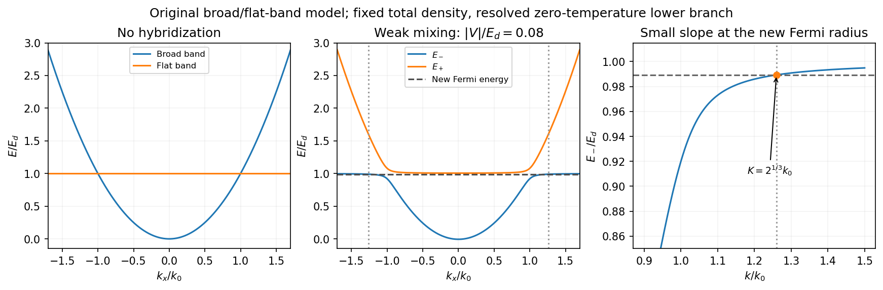
Uncoupled and weakly hybridized broad/flat bands, with the shifted Fermi radius and small lower-band slope
. Details. Fixed particle number and the larger Fermi sphere. Denote the uncoupled broad-band Fermi radius by to distinguish it from the new one . With two spin states, the broad-band number density at is . The stipulated equal population in the flat sector makes the total density twice that value. At zero temperature and any nonzero hybridization, all occupied states fit into the monotonic lower branch below , while the upper branch is empty. ThereforeThis is the stated factor increase. It uses fixed total particle number, equal spin counting, an exactly flat unhybridized band and enough available states below any Brillouin-zone restriction. In generic pairs of dispersive bands both hybridized pockets can remain occupied; then Fermi-volume conservation in two hybridized electron bands fixes a sum of volumes rather than this one radius. The exactly flat band is degenerate at , so its initial occupation must be specified, as it is here.
Fermi-velocity suppression. Set . The exact derivative of the lower branch isAt , and . For , the square bracket divided by two is . Since group velocity is and the broad-band reference velocity is ,so the flat-band hybridization Fermi-velocity suppression isThe reference velocity is that of the original broad-band Fermi sphere, not the broad-band slope at the larger ; omitting the radius change loses the factor .
The low-temperature qualification becomes more stringent as : the new chemical potential approaches with , and the relevant thermal energy must be small compared with this hybridization scale. At fixed nonzero temperature the singular flat-band redistribution is not automatically resolved for arbitrarily small coupling. A small but finite narrow-band dispersion can also change the occupation topology.
Density of states and magnetism. For an isotropic three-dimensional branch with spin degeneracy two,A small Fermi velocity therefore produces a large density of states. The localized, partially filled d-derived bands in iron, cobalt and nickel place many states close to the Fermi level; broad s/p-derived conduction bands in copper, silver and gold coexist with filled d bands lying below it. This explains the substantially larger Fermi-level density of states of the former group within the band picture. An exact factor of ten requires the actual band parameters and is not fixed by the two-band toy model.
A high density of states lowers the kinetic-energy cost of spin polarization. A repulsive exchange interaction can then satisfy the Stoner criterion and stabilize ferromagnetism. With a single-spin density of states and an on-site interaction normalization, the criterion is ; with spin-summed , it is . The large d-state contribution favors this instability in Fe, Co and Ni. The noble metals do not satisfy the corresponding instability condition in the same ordinary state; this does not imply that they have no weak magnetic response whatsoever.
Past exam of the quantum condensed matter course of the University of Cambridge 2014 2 c Solution Created 2026-10-18 Updated 2026-10-20
Both models respect Bloch's theorem and describe electrons in a periodic lattice, but they start from different useful limits.
In the nearly-free electron model, start with extended plane waves and free-electron energies . A weak periodic potential has Fourier coefficients at reciprocal lattice vectors and couples to . Away from degeneracies its corrections are small. Near a Bragg scattering, retain the two resonant plane waves and diagonalizeThe resulting eigenvalues areAt the crossing the gap is . The two standing-wave combinations place electronic density differently relative to the periodic potential and therefore acquire different energies. Folding the many free parabolas into the first Brillouin zone produces the repeated band labels; the nonzero potential opens avoided crossings between coupled states. A Fourier component forbidden by symmetry need not open its corresponding first-order gap.
In the tight-binding model, instead start with localized orbitals on well-separated atoms or sites, with discrete on-site energies. Their overlap permits tunneling represented by hopping integrals. Bloch sums of these orbitals diagonalize the lattice translation symmetry. For one orthonormal orbital per site in a one-dimensional nearest-neighbor chain,The many initially degenerate copies of one atomic orbital broaden into a band. Other atomic orbitals or multiple sites per primitive cell produce additional bands; their hybridization creates bonding and antibonding combinations and may open gaps. For two orbitals per cell, one illustrative Hamiltonian iswith eigenvalues . This shows explicitly how two bands arise from the two cell degrees of freedom, even when the isolated sites have equal on-site energies.
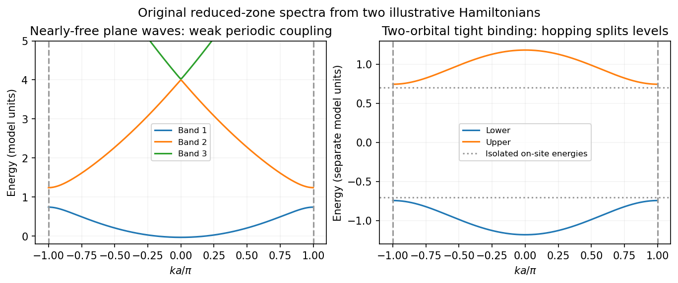
For each orbital degree of freedom per primitive cell there is one band per spin; band filling and the presence of a gap at the Fermi level determine metallic or insulating behavior. The nearly-free limit emphasizes weak Bragg scattering of extended states, while tight binding emphasizes hopping between localized states. They are complementary approximations to electronic band structure, rather than two incompatible explanations of why periodic solids have bands.
Past exam of the quantum condensed matter course of the University of Cambridge 2017 4 Solution Created 2026-10-18 Updated 2026-10-20
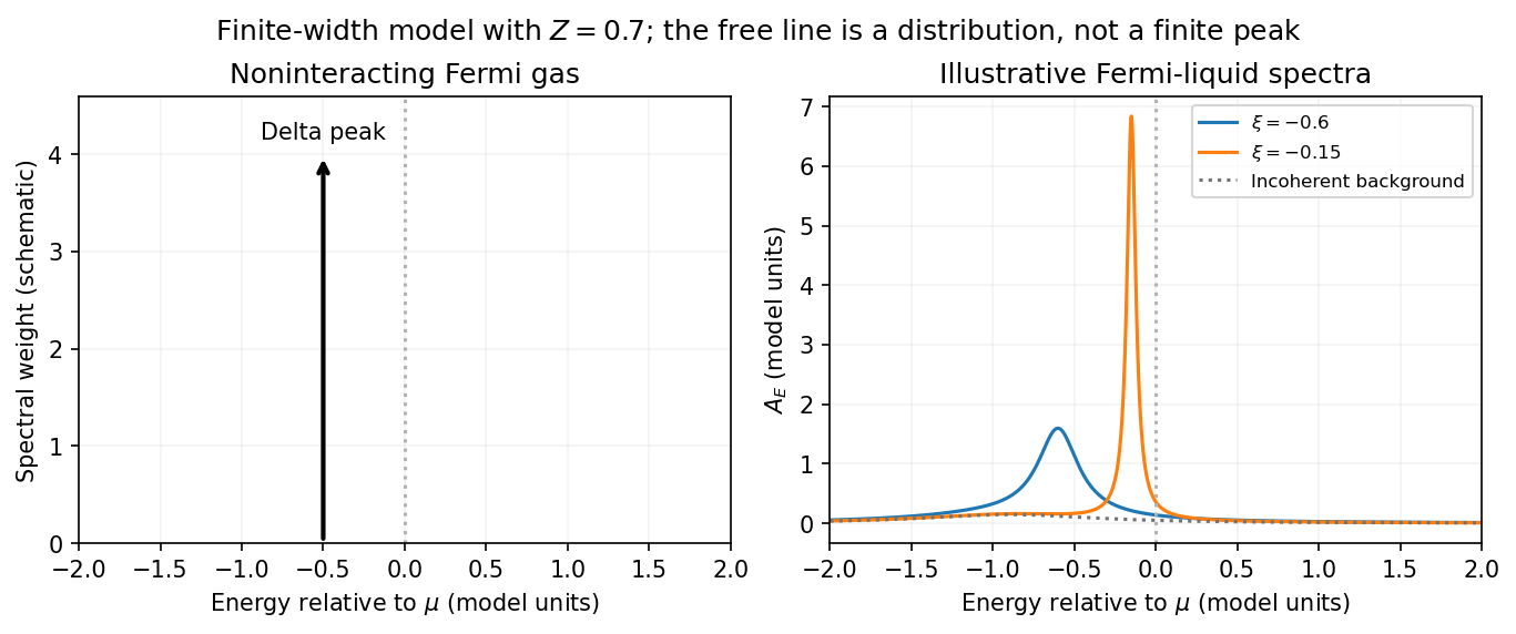
Noninteracting spectral line. Treat as a wavevector, so physical crystal momentum is . Write ; an energy zero at the chemical potential can be chosen throughout. The temporal factor of a noninteracting state is . With the Fourier transform convention ,Thus its normalized frequency spectral function isOne should not square the delta distribution as if it were an ordinary finite-time transition amplitude. More precisely, the fermionic retarded Green function is . Its Fourier transform is , whose negative imaginary part divided by is the same delta peak.
Interactions and lifetime. Interactions change the dispersion through the real part of the self-energy and permit decay into other excitations through its imaginary part. In the simplest quasiparticle-pole model, exponential decay of the retarded amplitude givesPerforming the causal integral,The corresponding Lorentzian quasiparticle spectral peak isIts total frequency integral is one. The exponential amplitude lifetime is ; the probability lifetime is . Describing as a scattering rate therefore requires the lifetime convention to be specified. The energy half-width is .
A general interacting electron is more accurately described by near the pole. The coherent peak then integrates to the quasiparticle residue and an incoherent continuum carries the remaining weight. In an energy-unit self-energy convention,Linearizing the real denominator gives and at the pole. The requested unit-weight Lorentzian is the normalized quasiparticle model, not the most general exact interacting spectrum.
Peak position and width. At fixed , put and . Differentiation givesIt is positive for and negative for , so the only maximum is at , with height . Setting to half this height gives . ThereforeIn energy units the maximum is and the half-width is . Frequency dependence of the self-energy would require reconsidering both the shape and peak position.
Fermi gas and Fermi liquid. A noninteracting Fermi gas has a delta-function spectral line at its bare dispersion for every momentum. A normal three-dimensional Fermi liquid has a shifted coherent peak plus incoherent spectral weight; close to the Fermi surface its width scales as . At zero temperature the peak becomes arbitrarily sharp at the Fermi surface, while it broadens farther away. Spectral functions include addition and removal weight; occupied-only photoemission contains an extra Fermi factor.


Photoemission measurement. A photon of known energy ejects an electron. Measure its kinetic energy and emission direction. For binding energy below the Fermi level and the appropriate calibrated work function , conservation of energy givesConservation of momentum parallel to a periodic surface giveswhere is a surface reciprocal-lattice vector. At suitable photon energies the photon momentum can be neglected; at higher energies it must be retained. The surface breaks perpendicular translation symmetry, so the perpendicular crystal momentum generally needs a final-state model. A two-dimensional band can be reconstructed directly from the parallel components.
Within the sudden approximation and electric-dipole approximation, photoemission intensity and spectral function are related byHere is measured relative to the chemical potential. Instrumental resolution convolves the product and inelastic scattering adds background. Thus ARPES maps the occupied electron removal spectral function, weighted by a matrix element; it does not measure the full unoccupied spectrum or an unweighted spectral function automatically. Bright ridges give dispersions, and intrinsic widths give decay information after instrumental effects are removed.
Reading the supplied image. Its bright ridges form a graphene-like cone. The crossing near is the Dirac point, not in general the Fermi level. In the paper's plotted energy coordinates its energy is roughly –. A velocity follows from a branch slope independently of the energy zero:For example, the lower branch moves by about between and . This gives andReading other points changes the estimate by tens of percent. The original exam image has unequal energy increments on nearly equally spaced labelled ticks, so it does not justify a precise fitted velocity. The value is an estimate of the cone slope extrapolated to the Fermi crossing, rather than a measured derivative exactly at a visibly identified Fermi cutoff.
To determine a Fermi energy, first calibrate the Fermi edge, then subtract the chosen reference energy. Neither a Fermi-level marker nor an explicit energy-zero convention is supplied in this crop. If its upper termination near is intended to represent the Fermi cutoff, the conditional graph answer is on that axis, or relative to the Dirac crossing. Identifying the crossing itself as the Fermi energy would incorrectly assume undoped graphene.
The research article cited by the exam identifies this as linearly polarized graphene ARPES and independently states for the substrate-doped sample. That resolves the relative energy when this external calibration is admitted.[ref]
https://hrg.pusan.ac.kr/articles/JPCM_0953-8984_26_33_335501.pdf. Section 3, printed p.2 and figure 1(b): Dirac point below the Fermi energy
The crop alone does not uniquely fix an absolute Fermi energy; the source-supported relative value and the conditional axis reading should be distinguished. Past exam of the quantum condensed matter course of the University of Cambridge 2018 Section A 1 b Solution Created 2026-10-18 Updated 2026-10-20
A positive gate voltage attracts electrons towards the oxide interface of the p-type semiconductor and repels mobile electron holes. The uncovered ionized acceptors form a negatively charged depletion region. Increasing the voltage further creates a thin electron-rich semiconductor inversion layer at the surface. The conduction band and valence band both bend downwards towards the positively biased gate, because an electron's electrostatic energy is .
In an ideal nondegenerate substrate with acceptor density , write and surface potential relative to the neutral bulk. The electron and hole surface densities areThe first change of majority-carrier type occurs at , where . The conventional MOS inversion threshold for appreciable strong inversion isAt threshold the inversion sheet is just developing, while a much thicker depletion region lies between it and the neutral p-type bulk. Inversion does not require the conduction band to cross the Fermi level: the surface can remain nondegenerate.
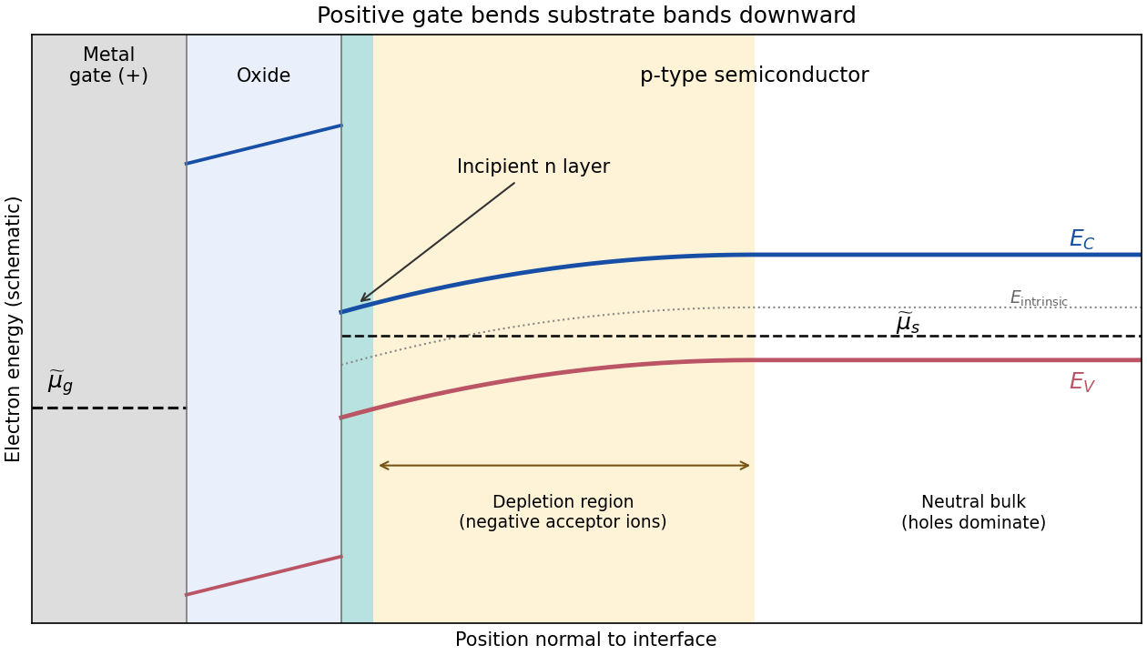

The metal and semiconductor Fermi levels need not be equal. The ideal oxide blocks particle exchange, so the gate and substrate can maintain different electrochemical potentials. In a biased MOSFET, the gate-to-substrate Fermi-level difference is , when the applied voltage is defined in the electron-reservoir convention. Each region can separately be in internal equilibrium. If an external zero-voltage connection instead equilibrates the reservoirs, their Fermi levels coincide, but different work functions can still cause band bending. Here the chemical potential shown in a band diagram is the electron electrochemical potential; the purely chemical contribution alone is not the equilibrium criterion for charged particles.